
Color film substrate and manufacture method and display device thereof

A technology of color film substrate and manufacturing method, which is applied in nonlinear optics, instruments, optics, etc., can solve the problems of high production cost, large number of mask plates, etc., and achieve the effect of position matching

Active Publication Date: 2016-03-16
BOE TECH GRP CO LTD +1
View PDF5 Cites 4 Cited by
  • Summary
  • Abstract
  • Description
  • Claims
  • Application Information

AI Technical Summary

Problems solved by technology

Currently, in the production process of color filter substrates, different masks are usually used to manufacture the black matrix 2 and color-resist blocks 3 of different colors. For example, when the color filter substrate includes sub-pixels of red, green and blue When making the black matrix, red color-resist block, green color-resist block, and blue color-resist block, each use a mask for exposure, the number of masks used is large, resulting in high production costs

Method used


Image

  • Color film substrate and manufacture method and display device thereof
  • Color film substrate and manufacture method and display device thereof
  • Color film substrate and manufacture method and display device thereof

Examples


Embodiment Construction

[0044] Specific embodiments of the present invention will be described in detail below in conjunction with the accompanying drawings. It should be understood that the specific embodiments described here are only used to illustrate and explain the present invention, and are not intended to limit the present invention.

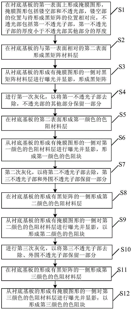
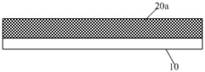
[0045] As one aspect of the present invention, a method for manufacturing a color filter substrate is provided, figure 2 It is a flow chart of the manufacturing method of the color filter substrate provided by the present invention, Figure 3 to Figure 20 is a schematic diagram of the manufacturing process of the color filter substrate, please refer to Figure 2 to Figure 20 , the color filter substrate includes multiple sub-pixel regions of different colors, and the manufacturing method includes:

[0046] S1. Form a mask pattern on the first surface of the base substrate 10, the mask pattern includes a hollow part 25 and an opaque part, the position of the h...


PUM

PropertyMeasurementUnit
transmittivityaaaaaaaaaa

Abstract

The invention provides a manufacture method of a color film substrate. The manufacture method comprises the steps that a masking pattern is formed on a first surface of a substrate, and comprises a hollowed-out part and a lightproof part, the lightproof part comprises a first lightproof subpart, the thickness of the first lightproof subpart is less than that of other parts of the lightproof part; a black matrix material layer is formed on a second surface of the substrate; the black matrix material layer is exposed and developed from one side where the masking pattern is formed, so that a black matrix is formed; ashing is performed for the first time to remove the first lightproof subpart, and one part of the other parts of the lightproof part is kept; a color resistance material layer of a first color is formed on the second surface of the substrate; the color resistance material layer of the first color is exposed and developed from one side where the masking pattern is formed, so that a color resistance block of the first color is formed. Correspondingly, the invention also provides a color film substrate and a display device. Through the invention, the usage quantity of mask plates can be reduced, and the production cost is lowered.

Description

technical field [0001] The invention relates to the field of display technology, in particular to a color filter substrate, a manufacturing method thereof, and a display device. Background technique [0002] The liquid crystal display panel includes an array substrate and a color filter substrate boxed together, and a liquid crystal layer located between the array substrate and the color filter substrate. Such as figure 1 As shown, the color filter substrate includes a base substrate 1 , a black matrix 2 and color-resist blocks 3 of various colors, and each sub-pixel area of ​​the color filter substrate is provided with a color-resist block 3 of a corresponding color. Currently, in the production process of color filter substrates, different masks are usually used to manufacture the black matrix 2 and color-resist blocks 3 of different colors. For example, when the color filter substrate includes sub-pixels of red, green and blue When making the black matrix, red color-res...

Claims


Application Information

Patent Timeline
Patent Type & Authority Applications(China)
IPC IPC(8): G02F1/1335
CPCG02F1/133512G02F1/133516
Inventor 陈曦刘明悬刘正刘耀张小祥张治超
Owner BOE TECH GRP CO LTD
Learn More