Shift register and driving method thereof, grid driving circuit, and display apparatus

A technology for shift registers and display devices, which is applied in static memory, digital memory information, instruments, etc., and can solve problems such as complex connection structure, increased process difficulty, and uncompetitive display panels.

Active Publication Date: 2016-03-23
BOE TECH GRP CO LTD
View PDF3 Cites 13 Cited by
  • Summary
  • Abstract
  • Description
  • Claims
  • Application Information

AI Technical Summary

Problems solved by technology

At present, although the output of the scanning signal can be realized by inputting more control signals with different functions, this makes the number of switching transistors forming the shift registers of each level in the gate driving circuit larger, and the gap between the switching transistors The specific structure of the connection is also relatively complicated, which increases the difficulty of the process and increases the production cost. Even because more signal lines are needed to input signals with different functions into the shift registers at all levels, the aperture ratio of the display panel is reduced. making the display panel uncompetitive

Method used


Image

  • Shift register and driving method thereof, grid driving circuit, and display apparatus
  • Shift register and driving method thereof, grid driving circuit, and display apparatus
  • Shift register and driving method thereof, grid driving circuit, and display apparatus

Examples


Embodiment 1

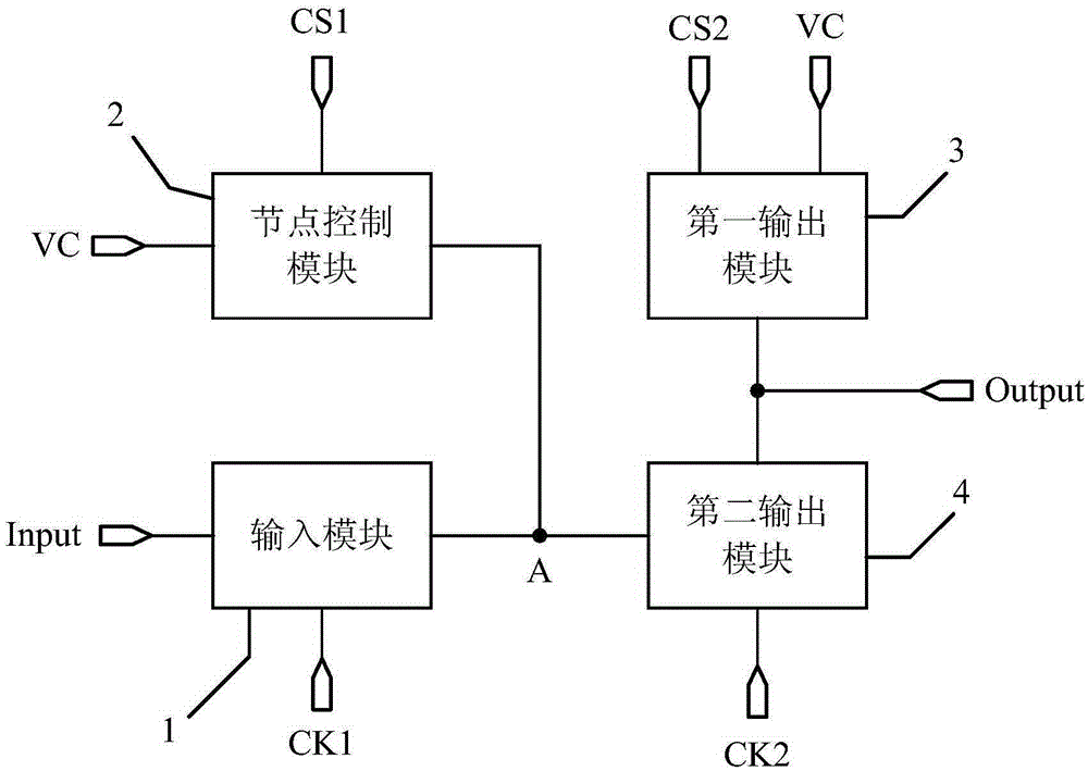
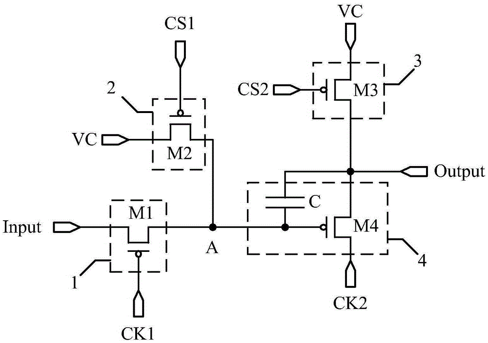
[0082] by Figure 2d The structure of the shift register shown is taken as an example to describe its working process, in which Figure 2d In the shift register shown, all switching transistors are P-type switching transistors, and each P-type switching transistor is turned on under the action of a low potential, and is turned off under the action of a high potential; the potential of the DC signal terminal VC is a high potential, and the corresponding The input and output timing diagram is as follows Figure 4a Shown, specifically, select as Figure 4a There are four stages in the shown input-output timing diagram, the first stage T1, the second stage T2, the third stage T3 and the fourth stage T4.

[0083] In the first stage T1, Input=1, CK1=1, CK2=0, CS1=0. Since CK1=1, the first switch transistor M1 is turned off; because CS1=0, both the second switch transistor M2 and the third switch transistor M3 are turned on; The signal of VC is provided to the first node A, so th...

Embodiment 2

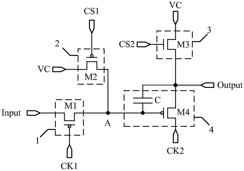
[0094] by Figure 3d The structure of the shift register shown is taken as an example to describe its working process, in which Figure 3d In the shift register shown, all switching transistors are N-type switching transistors, and each N-type switching transistor is turned on under the action of a high potential, and is turned off under the action of a low potential; the potential of the DC signal terminal VC is a low potential, and the corresponding The input and output timing diagram is as follows Figure 4b Shown, specifically, select as Figure 4b There are four stages in the shown input-output timing diagram, the first stage T1, the second stage T2, the third stage T3 and the fourth stage T4.

[0095] In the first stage T1, Input=0, CK1=0, CK2=1, CS1=1. Since CK1=0, the first switch transistor M1 is turned off; because CS1=1, both the second switch transistor M2 and the third switch transistor M3 are turned on; The signal of VC is provided to the first node A, so the...


PUM


Abstract

The invention discloses a shift register and a driving method thereof, a grid driving circuit, and a display apparatus. The shift register comprises an input module, a node control module, a first output module and a second output module. The input module controls potential of a first node through an input signal end and a first clock signal end, the node control module controls potential of the first node through a first control signal end and a DC signal end, the first output module controls potential of a driving signal output end through a second control signal end and the DC signal end, and the second output module maintains a stable voltage difference between the first node and the driving signal output end when the first node is at a floating state and controls potential of the driving signal output end through the first node and the second clock signal end. In such a way, through cooperation among the four modules, scanning signals can be output through a simple structure and fewer signal lines, the preparation process is simplified, and the production cost is decreased.

Description

technical field [0001] The invention relates to the field of display technology, in particular to a shift register, a driving method thereof, a gate driving circuit and a display device. Background technique [0002] With the rapid development of display technology, displays are increasingly developing toward high integration and low cost. Among them, the array substrate line drive (GateDriveronArray, GOA) technology integrates the thin film transistor (ThinFilmTransistor, TFT) gate switch circuit on the array substrate of the display panel to form a scan drive for the display panel, so that the gate integrated circuit ( Integrated Circuit (IC) bonding (Bonding) area and fan-out (Fan-out) area wiring space can not only reduce product cost in terms of material cost and manufacturing process, but also make the display panel symmetrical on both sides and narrow frame In addition, this integration process can also save the Bonding process in the direction of the gate scanning l...

Claims


Application Information

Patent Timeline
Patent Type & Authority Applications(China)
IPC IPC(8): G09G3/20G11C19/28
CPCG09G3/20G11C19/28G09G2300/0408G11C19/287G09G3/3266G09G2310/0286G09G2300/0465G09G2300/0426G09G3/3677
Inventor 马占洁
Owner BOE TECH GRP CO LTD
Why Eureka
Try Eureka