Supercharge Your Innovation With Domain-Expert AI Agents!

Polished sample comprising multiple wafer samples and method of preparation

A sample and wafer technology, applied in the field of preparing polished samples containing multiple wafer samples, can solve problems such as difficulty in flat bonding of tiny samples, easily damaged samples, and small samples, saving labor costs and consumables costs, and improving the success rate , the effect of improving efficiency

Active Publication Date: 2018-06-22
SEMICON MFG INT (SHANGHAI) CORP
View PDF6 Cites 0 Cited by
  • Summary
  • Abstract
  • Description
  • Claims
  • Application Information

AI Technical Summary

Problems solved by technology

[0012] In the above-mentioned existing polishing methods, since the sample is very small and fragile, it is very easy to damage the sample during the process of picking up, transferring and polishing the sample, so the success rate of sample polishing is only 50%
[0013] Also, flat bonding of tiny samples is very difficult and only one sample can be prepared at a time
Therefore, for the analysis process of selecting multiple samples, it is necessary to repeat the above process many times, resulting in a lot of unnecessary duplication of labor

Method used


Image

  • Polished sample comprising multiple wafer samples and method of preparation
  • Polished sample comprising multiple wafer samples and method of preparation
  • Polished sample comprising multiple wafer samples and method of preparation

Examples


Embodiment Construction

[0030] In the following description, the present invention is described with reference to various examples. One skilled in the art will recognize, however, that the various embodiments may be practiced without one or more of the specific details, or with other alternative and / or additional methods, materials, or components. In other instances, well-known structures, materials, or operations are not shown or described in detail so as not to obscure aspects of the various embodiments of the invention. Similarly, for purposes of explanation, specific quantities, materials and configurations are set forth in order to provide a thorough understanding of embodiments of the invention. However, the invention may be practiced without these specific details. Furthermore, it should be understood that the various embodiments shown in the drawings are illustrative representations and are not necessarily drawn to scale.

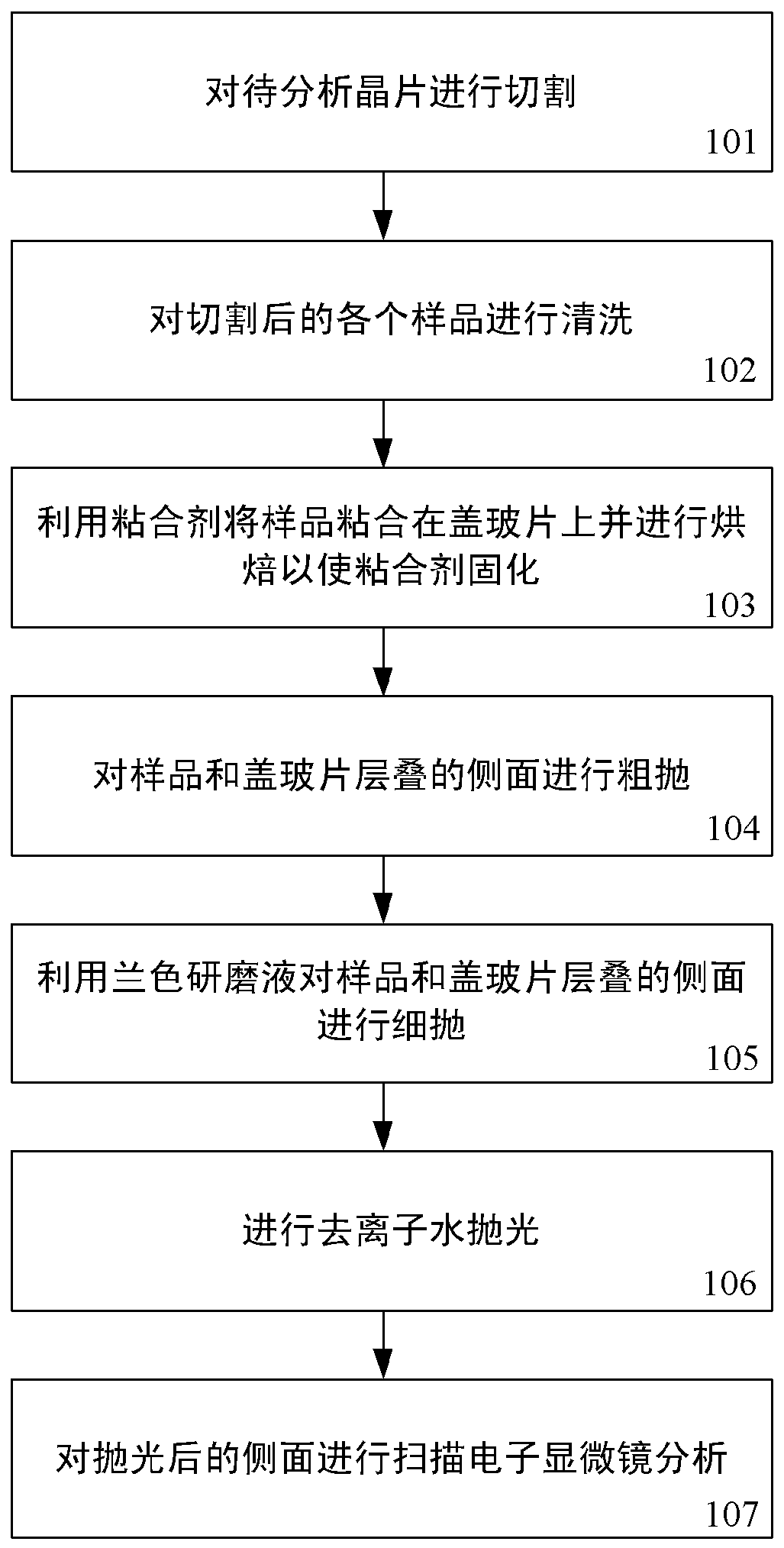
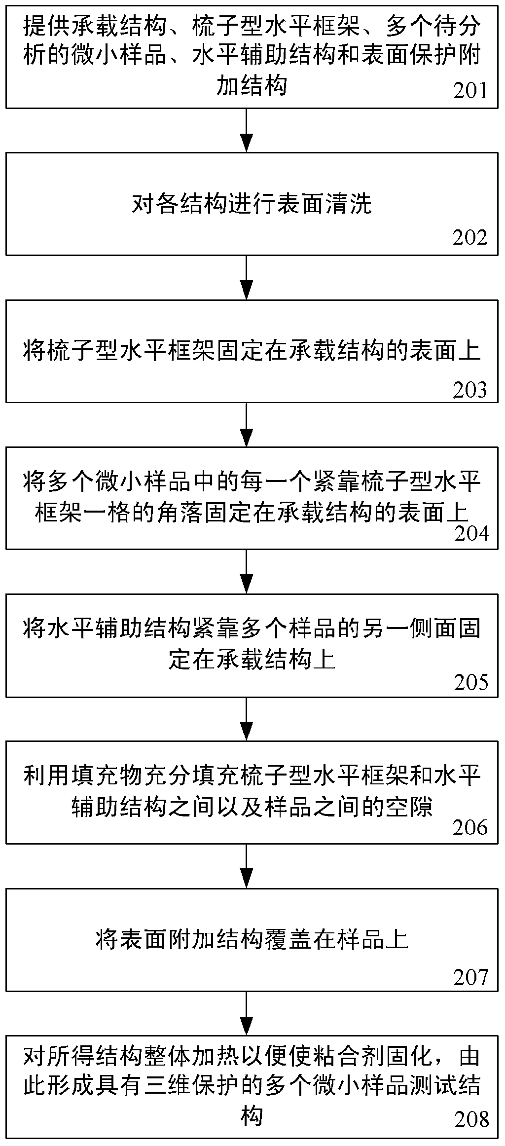
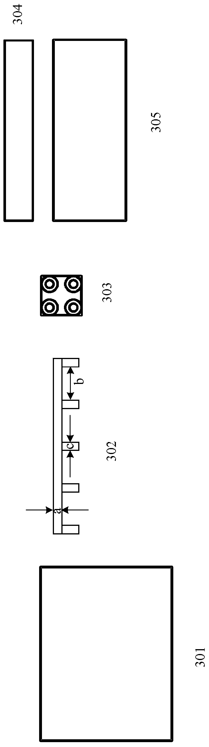
[0031] figure 2 A flowchart showing a polishing method for a plur...


PUM

PropertyMeasurementUnit
thicknessaaaaaaaaaa
thicknessaaaaaaaaaa
lengthaaaaaaaaaa

Abstract

The present invention discloses a polishing sample containing a plurality of wafer samples and a preparation method thereof, and the polishing sample can improve the polishing efficiency and the success rate of polishing of the wafer samples, and reduce the loss of materials. The polishing sample comprises a bearing structure, a comb-shaped horizontal frame, the plurality of wafer samples, a horizontal auxiliary structure, a filler and a surface protection additional structure, wherein the comb-shaped horizontal frame, the plurality of wafer samples and the horizontal auxiliary structure are on the bearing structure, the comb-shaped horizontal frame comprises a plurality of wafer sample grids defined by adjacent comb teeth, the filler is filled among the comb-shaped horizontal frame, the plurality of wafer samples and the horizontal auxiliary structure, the surface protection additional structure is on the comb-shaped horizontal frame, the plurality of wafer samples and the horizontal auxiliary structure, the plurality of wafer samples are clamped between the comb-shaped horizontal frame and the horizontal auxiliary structure, each of the plurality of wafer samples abuts against a corner of one corresponding wafer sample grid of the plurality of wafer sample grids, the heights of the comb-shaped horizontal frame and the horizontal auxiliary structure are less than or equal to the height of the plurality of wafer samples.

Description

technical field [0001] The invention relates to the field of manufacturing semiconductor devices, in particular to a method for preparing a polished sample containing a plurality of wafer samples and a structure obtained by the method. Background technique [0002] In the field of semiconductor technology, when using semiconductor technology to manufacture semiconductor devices, due to process defects in the semiconductor manufacturing process, such as metal particles introduced in the process, some semiconductor devices will have defects, so it is necessary to test and analyze the semiconductor devices to determine Whether the manufactured semiconductor device is a qualified product. [0003] At present, there are more and more analyzes of tiny samples, but conventional sample preparation methods usually cannot meet the requirements of sample analysis. For example, at present, a dedicated fully automated electron microscope sample thinning system (SELA) is usually used to ...

Claims


Application Information

Patent Timeline
Patent Type & Authority Patents(China)
IPC IPC(8): G01N1/32
Inventor 虞勤琴方君朱敏辛亚亚
Owner SEMICON MFG INT (SHANGHAI) CORP
Features
  • R&D
  • Intellectual Property
  • Life Sciences
  • Materials
  • Tech Scout
  • Unparalleled Data Quality
  • Higher Quality Content
  • 60% Fewer Hallucinations
Learn More