Printed wiring board and connector connecting said wiring board

A printed wiring board and wiring technology, applied in the direction of connection, printed circuit, printed circuit, etc., can solve the problems of not being able to obtain sufficient strength and difficulty in ensuring the retention of the wiring board, achieve excellent pull-out resistance, and eliminate ground short circuits Effect

Inactive Publication Date: 2016-04-13
FUJIKURA LTD +1
View PDF5 Cites 2 Cited by
  • Summary
  • Abstract
  • Description
  • Claims
  • Application Information

AI Technical Summary

Problems solved by technology

[0005] However, in the printed wiring board described in the above-mentioned Patent Document 1, the side where the slit is formed is composed only of a base film and a cover layer covering both surfaces of the base film, and these base films and cover layers are all made of a polyimide film. Therefore, if the thickness of the film becomes thinner with the further thinning and miniaturization of the printed wiring board, sufficient strength cannot be obtained around the cutout, and it is difficult to ensure sufficient holding of the connector to the printed wiring board force

Method used


Image

  • Printed wiring board and connector connecting said wiring board
  • Printed wiring board and connector connecting said wiring board
  • Printed wiring board and connector connecting said wiring board

Examples


Embodiment 1

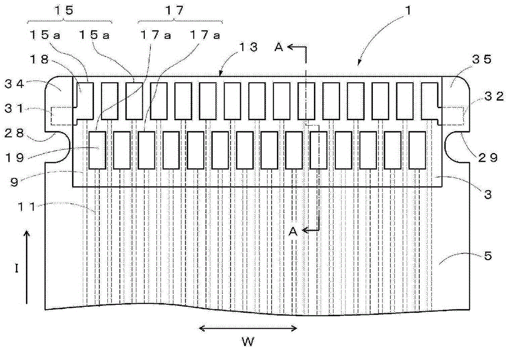
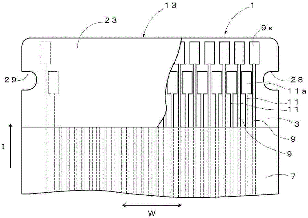
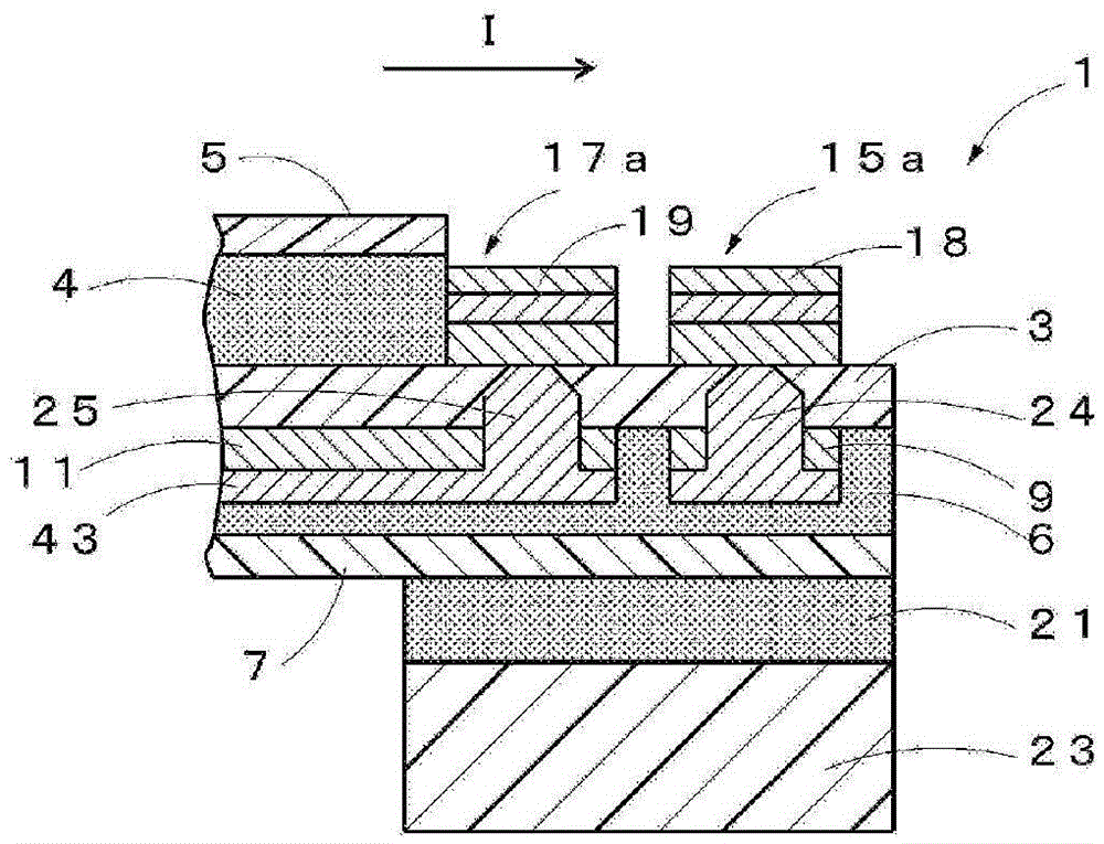
[0098] As Example 1, a trial production with Figure 1~4 The flexible printed wiring board of the structure shown. Specifically, the flexible printed wiring board has fifteen spacers in the front row and fourteen spacers in the back row at the connection end, and the space between the spacers is 0.175mm (0.35mm between each column). The surface (back surface) of the film on the opposite side to the surface on which the spacers are provided has the wiring of the spacers in the front row and the wiring of the spacers in the rear row, and is arranged on the front side and the front side of the notch (part to be engaged). Reinforcement layer integral with spacer. In addition, an insulating layer is formed on the upper surface of the reinforcement layer by the extending portion of the upper surface side covering layer. Spacers, wiring, and reinforcing layers are made of copper, and a gold-plated layer is formed on top of the spacers. As the base film, a film made of polyimide wi...

Embodiment 2

[0100] As Example 2, only as Figure 13 The shown flexible printed wiring board is different from Example 1 in that a reinforcement layer is formed independently on the upper surface side (the side where the spacer is formed) of the base film and does not have an insulating layer covering the reinforcement layer.

Embodiment 3

[0102] As Example 3, a trial production such as Figure 14 As shown, the flexible printed wiring board differs from Example 2 only in that it has the insulating layer which covers a reinforcing layer. Specifically, in the flexible printed wiring board of Example 3, the insulating layer covering the reinforcing layer is formed by the extended protrusion extending forward from the widthwise outer portion of the upper cover layer.


PUM


Abstract

This printed wiring board (1) is provided with: a base substrate (3); a plurality of pads (15a, 17a) for electrical connection disposed at one surface side of the base substrate (3) and for a connection terminal section (13) connecting to another electronic component (50); wiring (9, 11) connecting to the pads (15a, 17a); and engaged sections (28, 29) that are formed at the lateral edge section of the connection terminal section (13) and that are locked in the direction of disengagement to an engagement section (58) of the other electronic component (50). Also, the printed wiring board (1) is provided: with reinforcing layers (31, 32) formed integrally with pad (15a) and disposed at the one surface side of the base substrate (3) and at the front side of the engaged sections (28, 29) with respect to the connection direction to the other electronic component; and insulating layers (34, 35) covering the reinforcing layers (31, 32).

Description

technical field [0001] The present invention relates to a printed wiring board having a pad for electrical connection at a connection end portion connected to other electronic components such as a connector, and a connector for connecting the printed wiring board to another wiring board. Background technique [0002] Printed wiring boards are used to connect electronic components in electronic equipment such as digital cameras, digital video cameras, notebook computers, mobile phones, and game consoles. However, as such electronic equipment becomes lighter, thinner, and smaller, it is also required Thinning and miniaturization of the printed wiring board itself. However, if the printed wiring board is made thinner and smaller, the holding force of the connection end of the connector will decrease, and the connector will fall off or come into contact with the connector during installation due to the reaction force of the handling of the wiring or the impact of dropping. Bad ...

Claims


Application Information

Patent Timeline
Patent Type & Authority Applications(China)
IPC IPC(8): H05K1/11H01R12/77H01R12/88H05K1/02
CPCH01R12/77H01R12/88H05K1/117H05K2201/09036H05K2201/09063H05K2201/09409H01R12/73H05K1/111H05K2201/10189
Inventor 石田悠起铃木雅幸中野有贵浦井元德长江伦史
Owner FUJIKURA LTD
Why Eureka
Try Eureka