A jtag and bdm integrated debugging interface and its usage method

A technology for debugging interfaces and interfaces, applied in instruments, electrical digital data processing, computing, etc., can solve problems such as complex circuits, and achieve the effects of small circuit board area, convenient debugging, and high interface utilization.

Active Publication Date: 2018-03-30
DONGFENG COMML VEHICLE CO LTD
View PDF6 Cites 0 Cited by
  • Summary
  • Abstract
  • Description
  • Claims
  • Application Information

AI Technical Summary

Problems solved by technology

[0005] The purpose of the present invention is to overcome the problem of complicated circuits in the prior art, and provide a JTAG and BDM integrated debugging interface with simple circuits and its use method

Method used


Image

  • A jtag and bdm integrated debugging interface and its usage method
  • A jtag and bdm integrated debugging interface and its usage method
  • A jtag and bdm integrated debugging interface and its usage method

Examples


Embodiment 1

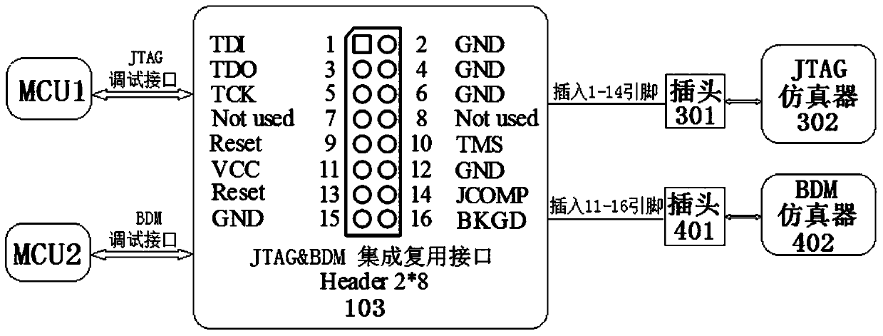
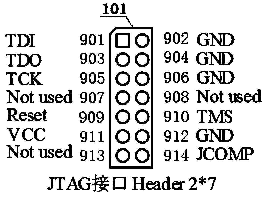
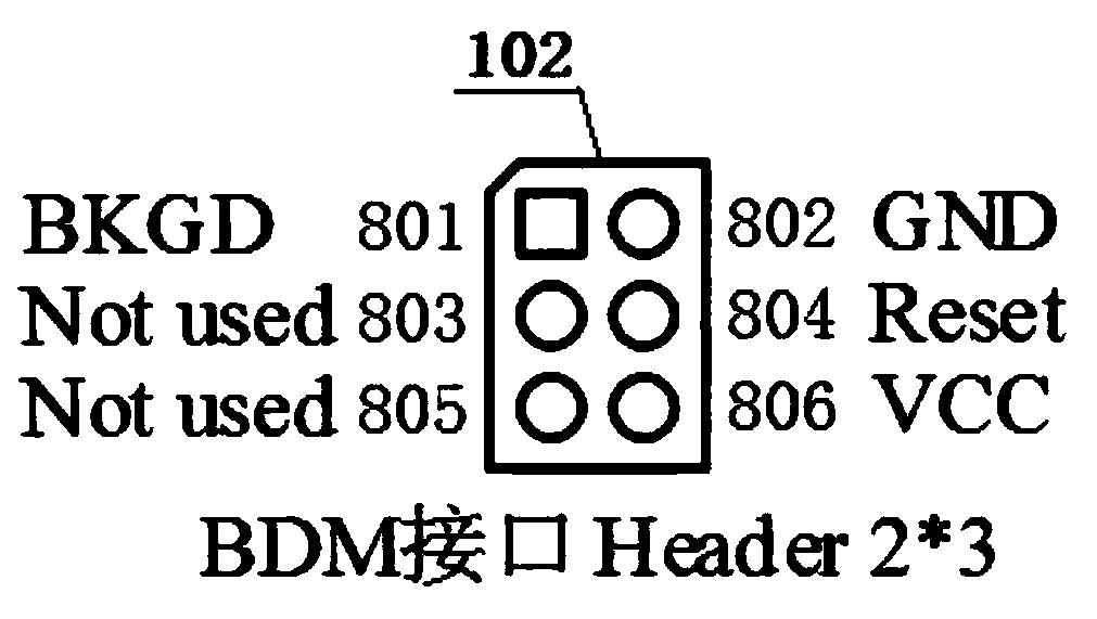
[0060] see figure 1 – Figure 5, a JTAG and BDM integrated debugging interface, including a JTAG interface 101 and a BDM interface 102, the JTAG interface 101 and the BDM interface 102 form a multiplexing debugging interface 103, and the multiplexing debugging interface 103 is two rows of symmetrically arranged pin headers interface, the multiplexing debug interface 103 is inserted and matched with the JTAG emulator plug 301 and the BDM emulator plug 401 respectively; the sum of the number of pins of the JTAG interface 101 and the number of pins of the BDM interface 102 is greater than or equal to multiplexing The number of pins of the debugging interface 103; the fourteen pins of the JTAG interface 101 are equally divided into left and right two columns for alignment, and the left column of the JTAG interface 101 has seven pins that are TDI901 pins from front to back. Pin, TDO903 pin, TCK905 pin, Not used907 pin, Reset909 pin, VCC911 pin and Not used913 pin, the seven pins o...


PUM


Abstract

The invention provides a JTAG and BDM integrated debugging interface and a using method thereof. The JTAG and BDM integrated debugging interface comprises a JTAG interface and a BDM interface, wherein the JTAG interface and the BDM interface form a multiplex debugging interface, the multiplex debugging interface includes two lines of pin interfaces in symmetrical arrangement, the multiplex debugging interface is in insertion matching with a JTAG emulator plug and a BDM emulator plug respectively. During use, the JTAG and BDM integrated debugging interface can be normally used by being directly inserted into a pin by being aligned to the pin. According to the design provided by the invention, not only is the multiplex of the JTAG interface and the BDM interface realized, but also the area of a circuit board is reduced and the material cost is saved.

Description

technical field [0001] The invention relates to a JTAG and BDM integrated multiplexing debugging interface of a Freescale (Freescale) MCU, in particular to a JTAG and BDM integrated debugging interface and a method of use thereof, and is particularly suitable for reducing the size of a circuit board and reducing the cost of an ECU. size and weight. Background technique [0002] The microcontroller or microprocessor in the embedded system has a debugging interface, which is used to connect with an emulator or a debugger for program flashing and debugging. The microcontrollers commonly used in the automotive industry mainly have two debugging interfaces, a 6pin BDM interface and a 14pin JTAG interface. When there are two microcontrollers on a circuit board and the debugging interfaces of the two microcontrollers are JTAG interface and BDM interface respectively, you need to use a 14pin connector (male end) and a 6pin connector on the circuit board respectively Connector (mal...

Claims


Application Information

Patent Timeline
Patent Type & Authority Patents(China)
IPC IPC(8): G06F11/267
CPCG06F11/267
Inventor 张志明
Owner DONGFENG COMML VEHICLE CO LTD
Why Eureka
Try Eureka