High-integration T component channel integration method for phased-array antenna

A phased array antenna, a high-integration technology, applied to antenna components, antennas, antenna arrays, etc., can solve the problems of phased array transmitting antenna spatial beamforming performance degradation, limited device installation space, and difficult integration methods. Achieve the effect of high-efficiency amplification, high reliability, and low technical difficulty

Inactive Publication Date: 2016-04-27
10TH RES INST OF CETC
View PDF2 Cites 11 Cited by
  • Summary
  • Abstract
  • Description
  • Claims
  • Application Information

AI Technical Summary

Benefits of technology

This patented technology improves on existing designs for achieving higher levels of performance (higher data transmission speed) while reducing energy usage compared to previous technologies like LC waveguides or hybrid circuits. It also allows more complex signal processing techniques such as digital predistortion and analog beamformers can now be used instead of expensive electronic equipment. Overall, this innovative solution helps improve communication systems' efficiency by enabling efficient use of limited resources within specific areas without sacrificing their functionality.

Problems solved by technology

Technics: Current designs for Ku-Band Phase Array Transmitted Antenna Units (KTA' s) use multiple separate parts such as transmitters, receivers, radiosets, and circuits related thereto. These parts require different types of materials like ceramic substrates, metal traces, dielectric layers, etc., resulting in increased manufacture costs due to material usage requirements and reduced overall device operational efficacy caused by heat dissipated during certain periods when they operate at frequencies below 1 GHz. To address these issues, there has been proposed various integrated methods involving combining several smaller subcomponents together into one larger unit while minimizing interference among themselves.

Method used


Image

  • High-integration T component channel integration method for phased-array antenna

Examples


Embodiment Construction

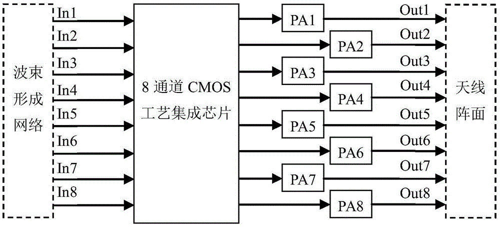
[0010] refer to figure 1 . In the embodiments described in the following embodiments, silicon-based CMOS technology is used to integrate chips according to the present invention, and multiple channels of Ka-band T components and multiple device functions of phase shifting and pre-amplification of each channel are integrated in silicon-based CMOS technology. In the integrated chip; then in the T component of the phased array transmitting antenna, the multi-channel Ka-band radio frequency signals from the beamforming network are sent to a multi-channel CMOS process integrated chip at the same time. Realize the phase shift, amplitude attenuation and power pre-amplification of multi-channel signals, and the multi-channel phase-shifted and amplified RF signals are output by the CMOS process integrated chip and sent to the corresponding number of corresponding power amplifier PA chips manufactured by GaAs process. , the power amplifier PA chip outputs the amplified Ka-band radio fr...


PUM


Abstract

The invention provides a high-integration T component channel integration method for a phased-array antenna, and aims at providing a high-integration and high-efficiency design method for an eight-channel T component, which is simple to achieve and can meet a Ka band. According to the technical scheme, multiple channels of a Ka-band T component and multiple phase-shifting and pre-amplifying device functions of each channel are integrated into a silicon-based CMOS process integration chip; in the T component of the phased-array transmitting antenna, multiple paths of Ka-band radio-frequency signals from a beam forming network are simultaneously transmitted into a multi-channel CMOS process integration chip and the silicon-based CMOS process integration chip; phase shifting, amplitude attenuation and power pre-amplification of the multiple paths of signals are achieved in parallel through a microcircuit; the CMOS process integration chip outputs multiple paths of phase-shifted and amplified radio-frequency signals to a gallium arsenide GaAs power amplifier PA chip; and the amplified Ka-band radio-frequency signals are output to multiple antenna array elements of an antenna array plane.

Description


Claims


Application Information

Patent Timeline
Owner 10TH RES INST OF CETC
Why Eureka
Try Eureka