Light emitting diode (LED) micro-array transparent display apparatus

A micro-array, transparent display technology, applied in the direction of electrical components, electric solid devices, circuits, etc., can solve the problem that the screen background or target cannot be displayed, the LED array is not transparent, the electrode material and substrate are not transparent, etc. problem, to achieve a good transparent display experience, high-quality transparent display function, light weight effect

Active Publication Date: 2016-05-04
GUANGDONG INST OF SEMICON IND TECH
View PDF4 Cites 8 Cited by
  • Summary
  • Abstract
  • Description
  • Claims
  • Application Information

AI Technical Summary

Problems solved by technology

However, the current LED arrays based on inorganic semiconductor materials do not have transparency, that is, they cannot display the background or objects behind the screen. The main reason is that the electrode materials and substrates used in traditional LED arrays do not have transparency.

Method used


Image

  • Light emitting diode (LED) micro-array transparent display apparatus
  • Light emitting diode (LED) micro-array transparent display apparatus
  • Light emitting diode (LED) micro-array transparent display apparatus

Examples


Embodiment 1

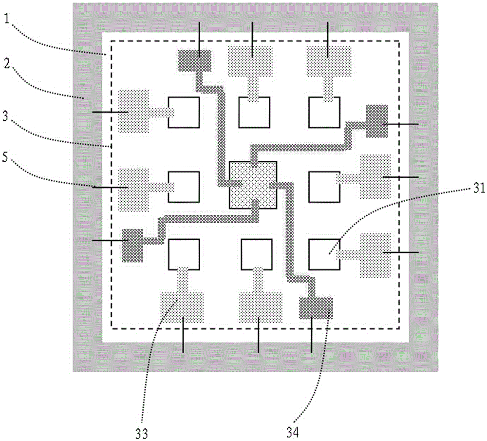
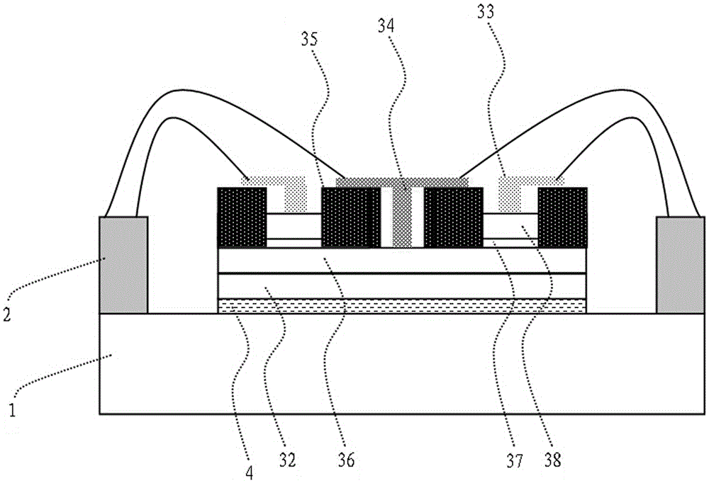
[0031] Such as Figure 1 to Figure 2 As shown, it is a LED micro-array transparent display device with independent addressing mode. The transparent display device includes a transparent substrate 1, a drive module 2 disposed on the transparent substrate 1, and a transparent inorganic semiconductor LED microarray 3, wherein the transparent inorganic semiconductor LED microarray 3 is tightly adhered to the transparent substrate by a transparent crystal bonding glue 4 1, the transparent substrate 1 surrounds the periphery of the transparent inorganic semiconductor LED micro-array 3, and the transparent p-type electrode 33 and the transparent n-type electrode 34 of the transparent inorganic semiconductor LED micro-array 3 are respectively driven by metal leads 5 and the transparent substrate 1. The modules 2 are connected so that the LED chips 31 of the transparent inorganic semiconductor LED micro-array 3 can be controlled to turn on and off through the driving module 2 . Moreov...

Embodiment 2

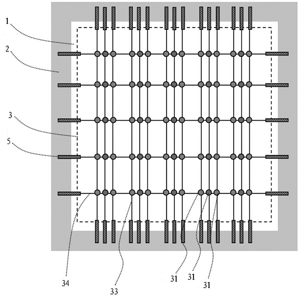
[0033] Such as Figure 3 to Figure 4 As shown, it is a LED micro-array transparent display device with a matrix addressing method. The transparent display device includes a transparent substrate 1, a drive module 2 disposed on the transparent substrate 1, and a transparent inorganic semiconductor LED microarray 3, wherein the transparent inorganic semiconductor LED microarray 3 has a matrix addressing electrode layout, that is, each column of LEDs The chip 31 shares the transparent p-type electrode 33, and the LED chips in each row share the transparent n-type electrode 34, and the transparent inorganic semiconductor LED micro-array 3 is tightly adhered to the center of the transparent substrate 1 through the transparent die-bonding glue 4, and the transparent substrate 1 surrounding the periphery of the transparent inorganic semiconductor LED micro-array 3 . The transparent die-bonding glue 4 is located between the transparent substrate 32 and the transparent substrate 1 . ...


PUM


Abstract

The invention relates to a light emitting diode (LED) micro-array transparent display apparatus. The apparatus comprises a transparent base board, a drive module and a transparent inorganic semiconductor LED micro-array that are arranged on the transparent base board. The drive module and the transparent inorganic semiconductor LED micro-array are electrically connected. Each LED chip of the transparent inorganic semiconductor LED micro-array can give out light from the front or a back transparent substrate or both the front and the back. The apparatus has high transparency and a good transparent display function, can display content that is programmable to some extent, and has flexible functions; the transparent display apparatus has a small size and light weight, meets the requirement of wearable devices on display, and is light and portable; in addition, the transparent display apparatus also has the advantages of high brightness, reliability and resolution and long service life, thereby bringing good transparent display experience; and the transparent display apparatus is realized through a standard semiconductor technology, is simple to prepare, and can be produced in a large scale.

Description

technical field [0001] The invention relates to the technical field of LED-based micro-displays, in particular to a LED micro-array transparent display device. Background technique [0002] Transparent display is a new generation of display technology that can display the background (object) behind the screen in addition to the basic display function. Its application fields include portable electronic consumer products, navigation equipment, collimators, helmet displays, Shop windows, information bulletin boards, etc., including Samsung and many other panel manufacturers are conducting research and development of transparent display technology. At present, conceptual transparent display products based on LCD or OLED have appeared in the market, but they have disadvantages such as high cost, low display brightness, and low transparency (30-40% transmittance). In addition, micro-display technology based on high-brightness, inorganic semiconductor material LED arrays (such as ...

Claims


Application Information

Patent Timeline
Patent Type & Authority Applications(China)
IPC IPC(8): H01L27/12
CPCH01L27/1214
Inventor 刘宁炀龚政陈志涛刘晓燕赵维任远
Owner GUANGDONG INST OF SEMICON IND TECH
Why Eureka
Try Eureka