Pixel array substrate

A pixel array substrate and substrate technology, which is applied to digital memory information, instruments, semiconductor devices, etc., can solve the problems of reducing the width of the frame and increasing the load of the GOA circuit, and achieve the effect of reducing the width of the peripheral area.

Active Publication Date: 2016-05-04
AU OPTRONICS CORP
View PDF5 Cites 15 Cited by
  • Summary
  • Abstract
  • Description
  • Claims
  • Application Information

AI Technical Summary

Problems solved by technology

However, in the existing GOA circuit, the bus lines of the GOA circuit occupy more than 40% of the overall width of the GOA circuit, which is not conducive to further reducing the frame width.
In addition, in order to arrange more lines in a limited area, the connection line of the GOA circuit often crosses the bus, and then couples with the bus to form a parasitic capacitance, which increases the load of the GOA circuit.

Method used


Image

  • Pixel array substrate
  • Pixel array substrate
  • Pixel array substrate

Examples


Embodiment Construction

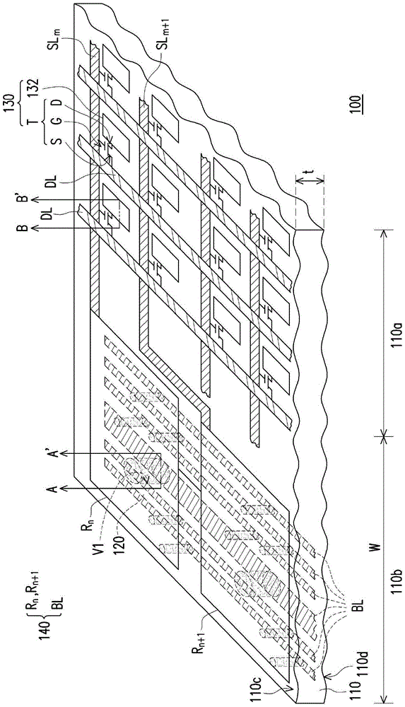
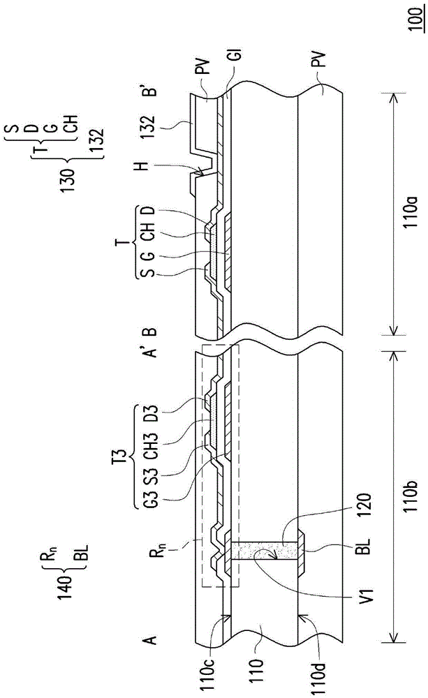
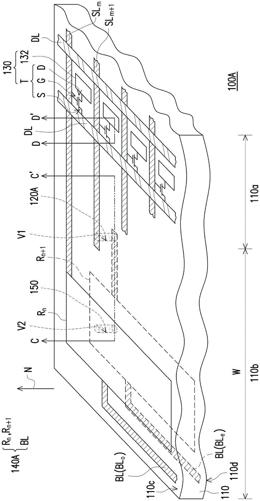
[0052] figure 1 It is a three-dimensional schematic diagram of a pixel array substrate according to an embodiment of the present invention. figure 2 It is a schematic cross-sectional view of a pixel array substrate according to an embodiment of the present invention. in particular, figure 2 corresponds to figure 1 The section line A-A', B-B'. Please refer to figure 1 , the pixel array substrate 100 includes a substrate 110, at least one conductive object 120, a plurality of pixel units 130, a plurality of data lines DL, and a plurality of scan lines SL m 、SL m+1 and a scan driving circuit 140 . The substrate 110 has a display area 110a, a peripheral area 110b outside the display area 110a, a first surface 110c, and a second surface 110d opposite to the first surface 110c. The peripheral area 110b of the substrate 110 is provided with at least one through hole V1 penetrating through the first and second surfaces 110c, 110d. In this embodiment, the through hole V1 can ...


PUM


Abstract

The invention discloses a pixel array substrate. The pixel array substrate comprises a substrate body with at least one penetrating hole, at least one conductive object disposed in the at least one penetrating hole, a plurality of pixel units, a plurality of scanning lines electrically connected with the pixel units, at least one shifting register and at least one bus. The pixel units, the scanning lines and the at least one shifting register are configured on a first surface of the substrate body. The at least one shifting register are used to transfer a first grid electrode signal to corresponding scanning lines. The at least one bus are disposed a second surface of the substrate body. The at least one bus pass through the at least one conductive object and are electrically connected with the at least one shifting register.

Description

technical field [0001] The present invention relates to an active component substrate, and in particular to a pixel array substrate. Background technique [0002] In recent years, the awareness of environmental protection has risen, and the flat display panel (flat display panel) with superior characteristics such as low power consumption and good space utilization efficiency has become the mainstream of the market. However, with the development of display technology, users have turned their focus to the aesthetic appearance of the display panel in addition to the above characteristics. In detail, users not only hope that the display panel has superior characteristics such as low power consumption and good space utilization efficiency, but also hopes that the display panel has a large display area and a narrow border (slimboarder), so as to realize a simple and elegant display. [0003] In order to realize a display panel with a narrow frame, it has been proposed that when ...

Claims


Application Information

Patent Timeline
Patent Type & Authority Applications(China)
IPC IPC(8): H01L27/12
CPCH01L27/1214H01L27/124G09G3/3648G09G2300/0408G09G2300/0426H01L27/1218H01L27/1251G11C19/28H01L29/78609
Inventor 卓伟民黄郁升陈嘉伟
Owner AU OPTRONICS CORP
Why Eureka
Try Eureka