Display tile structure and tiled display

a display and tile technology, applied in semiconductor devices, solid-state devices, instruments, etc., can solve the problems of limiting the size of integrated flat-panel devices such as displays, difficult and expensive thin-film semiconductor structures on large substrates, and crystalline semiconductors found in typical integrated circuits. achieve the effect of improving functionality, reducing thickness, and increasing resolution

Active Publication Date: 2017-02-16
X DISPLAY CO TECH LTD
View PDF5 Cites 91 Cited by
  • Summary
  • Abstract
  • Description
  • Claims
  • Application Information

AI Technical Summary

Benefits of technology

The present invention provides display tiles that can be integrated with a backplane to form a tiled display. The display tiles include inorganic light emitters, such as micro-LEDs, which are mounted to emit light in a direction opposite the backplane and have electrodes, micro-wires, and contact pads on a side of the light emitters opposite the direction of light emission. This arrangement simplifies the structure and construction of display tiles and more readily enables display tiles with a reduced perimeter width between the light emitters and the edge of the display tile that, in turn, can increase the resolution of the tiled display. Additionally, the present invention allows for increased display resolution and reduced manufacturing cost by providing display tiles that are formed using very small components, such as micro-LEDs and small interconnections. This was also enabled by reducing the required size of the display tiles and using low-resolution interconnections and additional circuitry that enhances the functionality of the display tiles. Overall, the present invention provides a display tile structure and tiled display with increased resolution, reduced thickness, improved functionality, and reduced manufacturing cost.

Problems solved by technology

However, the thin layer of semiconductor material is typically amorphous or has localized crystals, for example in amorphous silicon or polysilicon.
These semiconductor material structures have a much lower performance than crystalline semiconductors found in typical integrated circuits.
Moreover, it is difficult and expensive to make thin-film semiconductor structures on large substrates, limiting the size of integrated flat-panel devices such as displays.
Passive-matrix control structures that do not require a thin-film semiconductor layer are also known but are limited in size resolution, and refresh rate.
However, it is in general challenging to provide electrical interconnections to the pixels in the tiles and to maintain a constant pixel pitch across the tile boundaries.
However, this arrangement requires multiple substrates and the use of vias to connect integrated circuits on the driver substrate to the LED display substrate and is not suitable for a scalable tiled structure.
As discussed in U.S. Pat. No. 5,686,790, integrated circuits mounted on the light-emitting side of the backplane unnecessarily increase the size of the backplane while integrated circuits mounted on the side of the backplane opposite the light-emitting structures require electrical vias through the backplane or electrical leads wrapped around the edge of the backplane to electrically connect the integrated circuits with the light-emitting structures.
Such vias and leads are difficult and expensive to construct.
Integrated circuits located within the display area of a display reduce the resolution and aperture ratio of the display.
In flat-panel displays such as LCDs and OLEDs, a reduced aperture ratio also reduces the brightness or lifetime of the display.
However, these PCBs can be limited in the spatial resolution provided for integrated circuit electrical interconnections.
Daughter cards used in conjunction with motherboards (i.e., smaller printed circuit boards mounted upon and electrically connected to larger printed circuit boards) are also known but likewise have limited spatial resolution, orientation, and integration provided for integrated circuits.

Method used


Image

  • Display tile structure and tiled display
  • Display tile structure and tiled display
  • Display tile structure and tiled display

Examples


Embodiment Construction

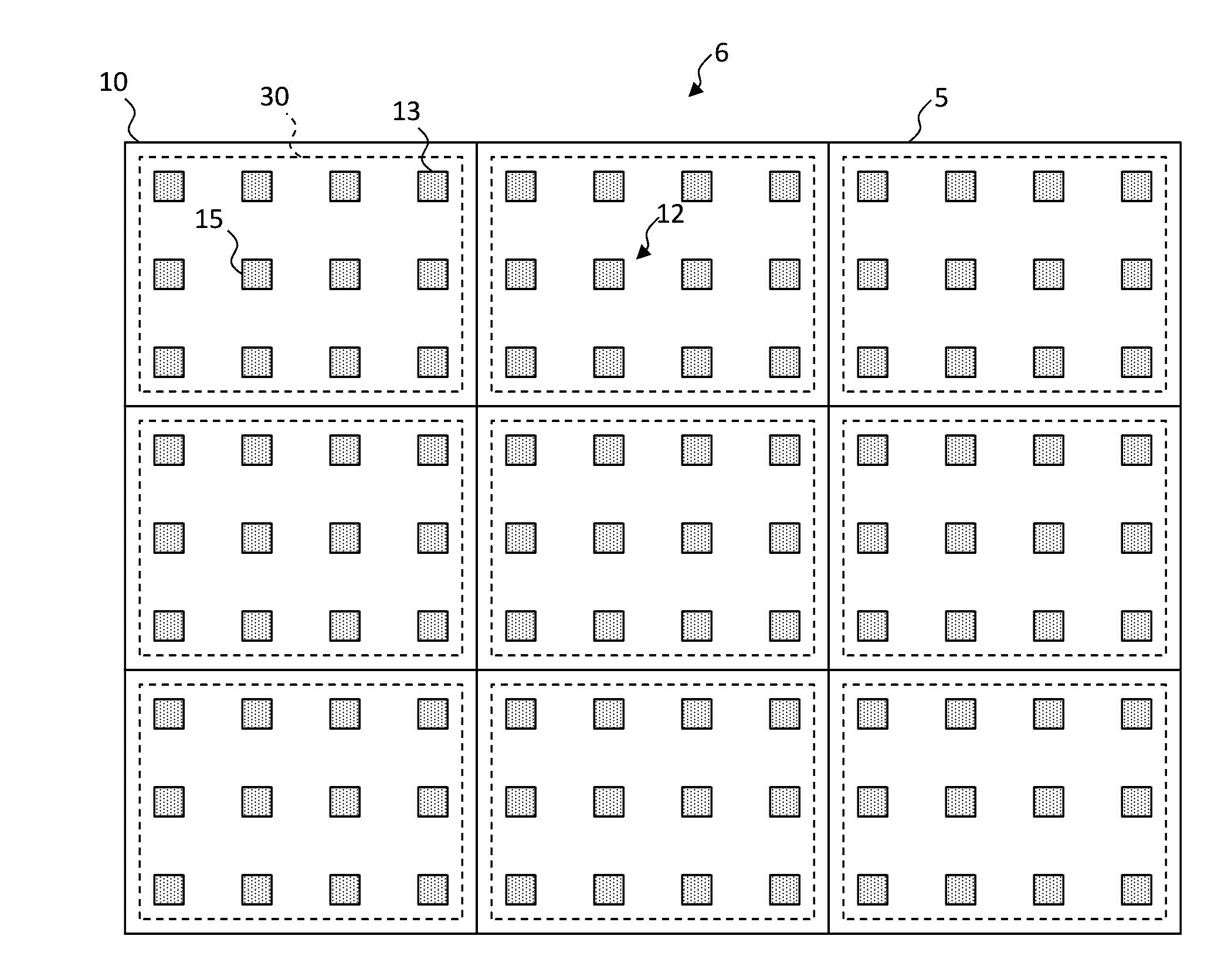
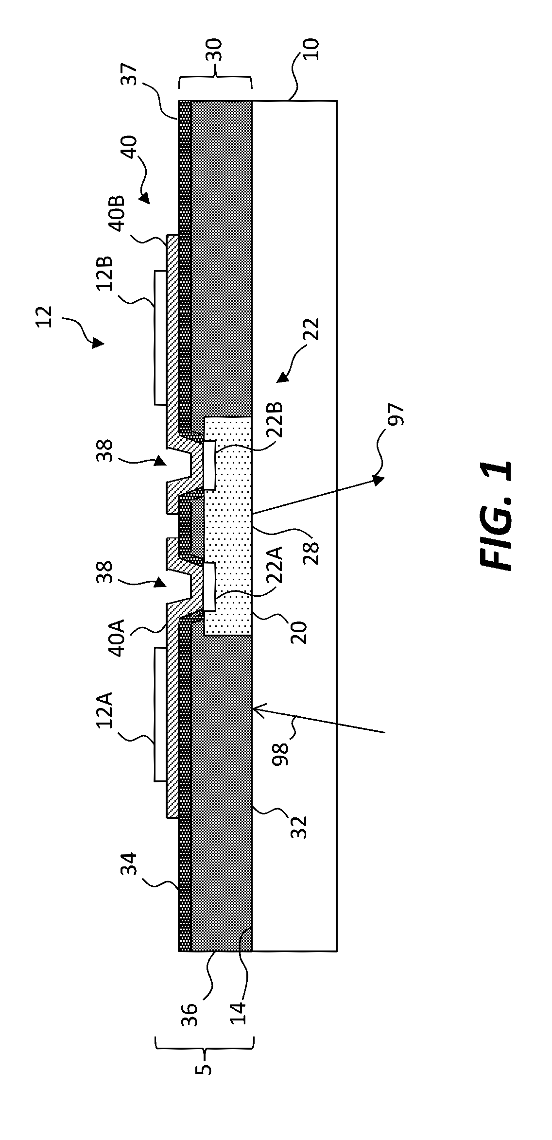
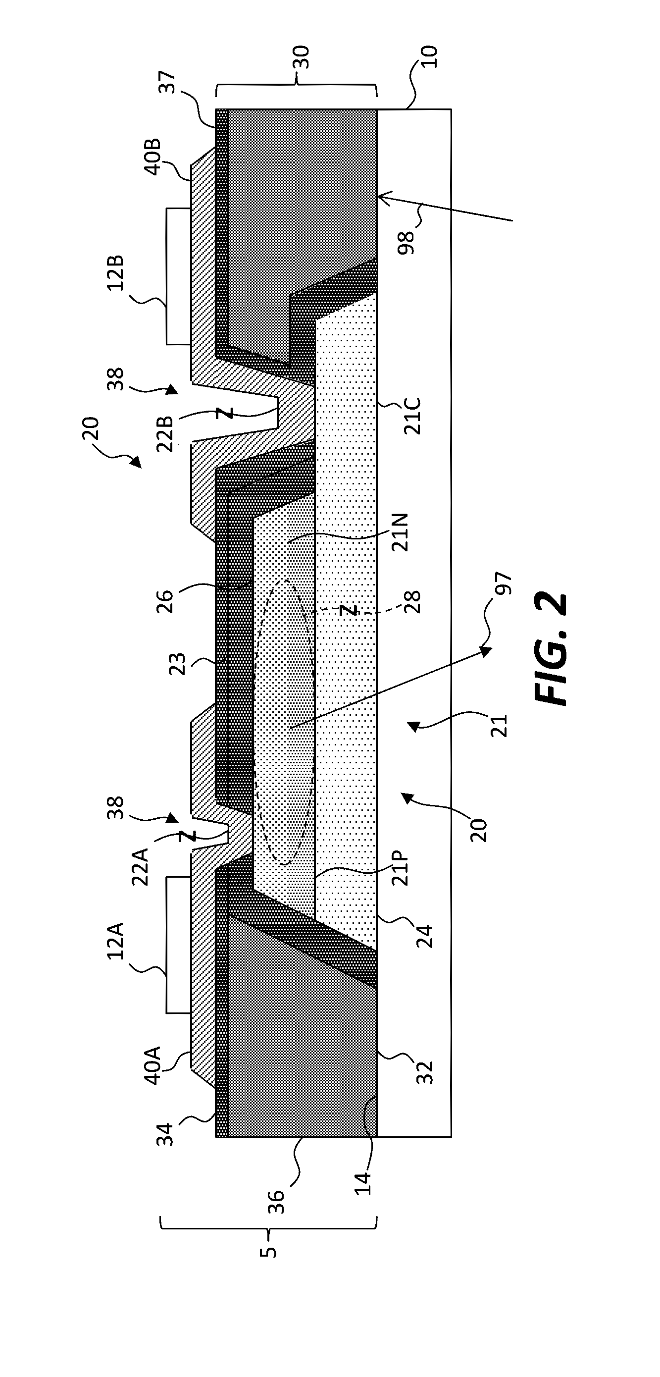
[0065]Referring to the cross section of FIG. 1 and the detailed cross section of FIG. 2, in an embodiment of the present invention a display tile structure 5 includes a tile layer 30 having a backplane side 34 and an emitter side 32 opposite the backplane side 34. The tile layer 30 can include or be a light-absorbing material 36 and can include sub-layers such as a dielectric layer 37, particularly if the tile layer 30 is at least partially electrically conductive. The dielectric layer 37 can be an interlayer dielectric. A light emitter 20 is disposed in the tile layer 30 and arranged to emit light 97 from a light-emitting area 28 on the emitter side 32 of the tile layer 30. The light emitter 20 has first and second electrodes 22A, 22B, collectively referred to as electrodes 22, for conducting electrical current to cause the light emitter 20 to emit light 97. The first and second electrodes 22A, 22B can also be considered to be first and second light-emitter contact pads for the lig...


PUM


Abstract

A display tile structure includes a tile layer with opposing emitter and backplane sides. A light emitter having first and second electrodes for conducting electrical current to cause the light emitter to emit light is disposed in the tile layer. First and second electrically conductive tile micro-wires and first and second conductive tile contact pads are electrically connected to the first and second tile micro-wires, respectively. The light emitter includes a plurality of semiconductor layers and the first and second electrodes are disposed on a common side of the semiconductor layers opposite the emitter side of the tile layer. The first and second tile micro-wires and first and second tile contact pads are disposed on the backplane side of the tile layer.

Description

CROSS REFERENCE TO RELATED APPLICATIONS[0001]Reference is made to commonly assigned U.S. patent application Ser. No. 14 / 807,259, filed Jul. 23, 2015 and entitled Redistribution Layer for Substrate Contacts by Bower et al, to commonly assigned U.S. patent application Ser. No. 14 / 743,984, filed Jun. 18, 2015 and entitled Systems and Methods for Preparing GaN and Related Materials for Micro Assembly by Bower et al, to commonly assigned U.S. patent application Ser. No. 14 / 807,311, filed Jul. 23, 2015 and entitled Printable Inorganic Semiconductor Method by Meitl et al, to commonly assigned U.S. patent application Ser. No. 14 / 818,201, filed Aug. 4, 2015 and entitled Inorganic-Light-Emitter Display with Integrated Black Matrix by Bower et al, to commonly assigned U.S. patent application Ser. No. 14 / 743,981, filed Jun. 18, 2015 and entitled Micro-Assembled Micro LED Displays and Lighting Elements by Bower et al, and to commonly assigned U.S. Patent Application Ser. No. 62 / 055,472 filed Sep...

Claims


Application Information

Patent Timeline
Patent Type & Authority Applications(United States)
IPC IPC(8): H01L27/32H01L25/04H01L51/56H01L33/62H01L33/64H01L51/52H01L25/075H01L27/15
CPCH01L27/3293H01L25/0753H01L25/048H01L27/156H01L27/3276H01L27/3288H01L2227/326H01L33/64H01L51/529H01L51/56H01L2933/0066H01L2933/0075H01L33/62H01L2224/18G06F3/04166G06F2203/04104G06F3/04164G06F3/042G06F3/044G06F3/0412H10K50/87H10K59/18H10K59/131H10K59/179H10K71/00H10K59/1201H10K71/80H10K59/90H01L33/58
Inventor BOWER, CHRISTOPHERMEITL, MATTHEWCOK, RONALD S.
Owner X DISPLAY CO TECH LTD
Why Eureka
Try Eureka