Pixel circuit and driving method thereof, and organic electroluminescent display panel

A pixel circuit and light-emitting device technology, applied in static indicators, instruments, etc., can solve the problems of affecting image display effect and uneven display brightness

Active Publication Date: 2016-05-11
BOE TECH GRP CO LTD
View PDF5 Cites 20 Cited by
  • Summary
  • Abstract
  • Description
  • Claims
  • Application Information

AI Technical Summary

Problems solved by technology

However, due to reasons such as technological process and device aging, the threshold voltage V of the driving transistor in the pixel circuit will be th There is i

Method used


Image

  • Pixel circuit and driving method thereof, and organic electroluminescent display panel
  • Pixel circuit and driving method thereof, and organic electroluminescent display panel
  • Pixel circuit and driving method thereof, and organic electroluminescent display panel

Examples


Embodiment 1

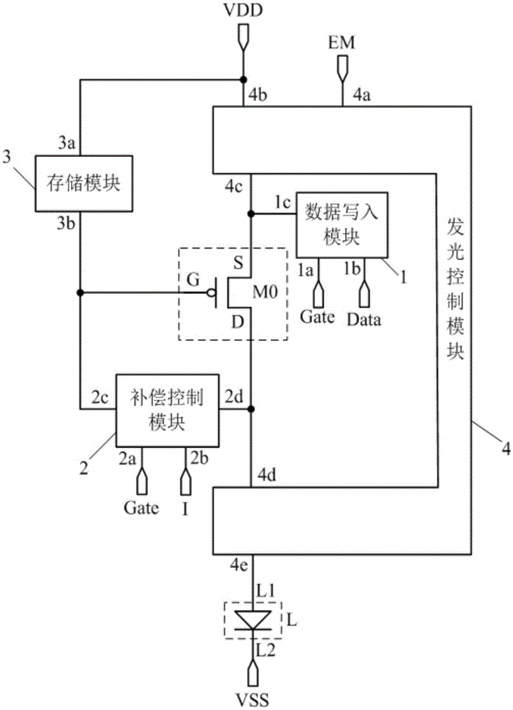
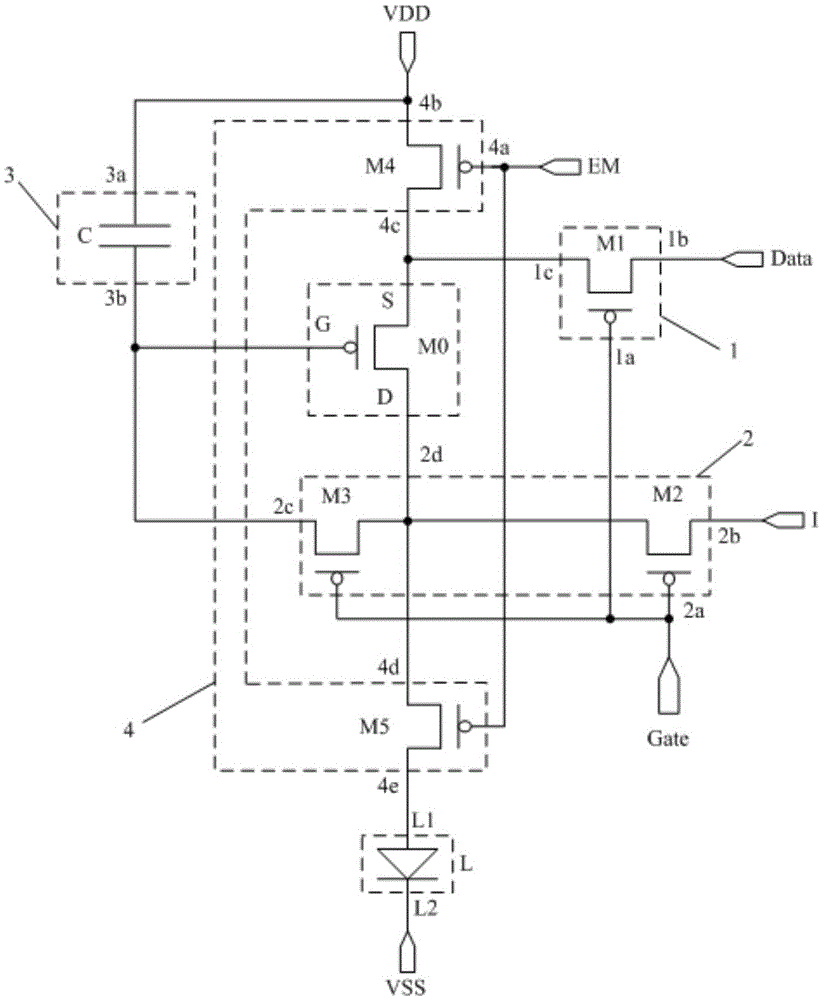
[0082] like Figure 2a As shown, the driving transistor M0 is a P-type transistor, and all switching transistors are P-type switching transistors; the corresponding circuit timing diagram is shown in Figure 4a As shown, it includes two stages: a compensation stage T1 and a light emitting stage T2.

[0083] In the compensation phase T1, Gate=0, EM=1, Data=1.

[0084] Since Gate=0, the first switch transistor M1 , the second switch transistor M2 and the third switch transistor M3 are all turned on; since EM=1, the fourth switch transistor M4 and the fifth switch transistor M5 are all turned off. The turned-on first switch transistor M1 converts the voltage V of the data signal terminal Data Data Provided to the source S of the drive transistor M0; the turned-on second switch transistor M2 provides the preset bias current I_Bias of the bias current terminal I to the source of the third switch transistor M3; the turned-on third switch transistor M3 The preset bias current I_Bi...

Embodiment 2

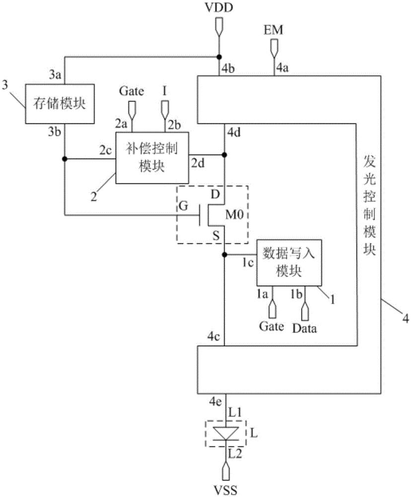
[0089] like Figure 3a As shown, the driving transistor M0 is an N-type transistor, and all switching transistors are N-type switching transistors; the corresponding circuit timing diagram is shown in Figure 4b As shown, it includes two stages: a compensation stage T1 and a light emitting stage T2.

[0090] In the compensation phase T1, Gate=1, EM=0, Data=1.

[0091] Since Gate=1, the first switch transistor M1 , the second switch transistor M2 and the third switch transistor M3 are all turned on; since EM=0, the fourth switch transistor M4 and the fifth switch transistor M5 are all turned off. The turned-on first switch transistor M1 converts the voltage V of the data signal terminal Data Data Provided to the source S of the drive transistor M0; the turned-on second switch transistor M2 provides the preset bias current I_Bias of the bias current terminal I to the source of the third switch transistor M3; the turned-on third switch transistor M3 Provide the preset bias cur...


PUM


Abstract

The invention discloses a pixel circuit and a driving method thereof, and an organic electroluminescent display panel. A driving transistor, a data writing-in module, a compensation control module, a storage module, a luminescence control module and a luminescent device are included. Through mutual cooperation of the above four modules, a work current of luminescence of the luminescent device driven by the driving transistor is unrelated to a threshold voltage of the driving transistor; an influence of drifting of the threshold voltage on the luminescent device can be avoided so that the work current used for driving the luminescent device to carry out luminescence can keep stable and uniformity of image display brightness is increased.

Description

technical field [0001] The invention relates to the field of display technology, in particular to a pixel circuit, a driving method thereof and an organic electroluminescent display panel. Background technique [0002] Organic Light-Emitting Diode (OLED) is one of the hotspots in the field of flat panel display research today. Compared with Liquid Crystal Display (LCD), OLED has fast response, high brightness, high contrast, low power consumption and easy flexibility. Display and other advantages, is considered to be the next generation of mainstream displays. Among them, the pixel circuit is the core technical content of the OLED display, which has important research significance. Unlike LCD, which uses a stable voltage to control brightness, OLED is current-driven and requires a stable current to control light emission. However, due to reasons such as technological process and device aging, the threshold voltage V of the driving transistor in the pixel circuit will be t...

Claims


Application Information

Patent Timeline
IPC IPC(8): G09G3/3208G09G3/3233
CPCG09G3/3208G09G3/3233G09G2300/0842G09G2300/0861G09G2300/0819G09G2320/0233G09G2320/045G09G3/3266G09G3/3275
Inventor 马占洁
Owner BOE TECH GRP CO LTD
Why Eureka
Try Eureka