
Fingerprint sensor

A fingerprint sensor and fingerprint signal technology, applied in the field of sensors, can solve the problems such as the inability to improve the length of the amorphous silicon glass panel and the flexible circuit board 24, and increase the area of ​​the substrate product, so as to save the glue bonding area and save the The effect of reducing the area and reducing the cost of device manufacturing

Active Publication Date: 2016-05-25
SHANGHAI OXI TECH
View PDF3 Cites 2 Cited by
  • Summary
  • Abstract
  • Description
  • Claims
  • Application Information

AI Technical Summary

Problems solved by technology

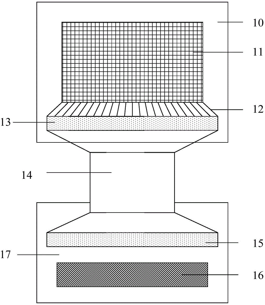
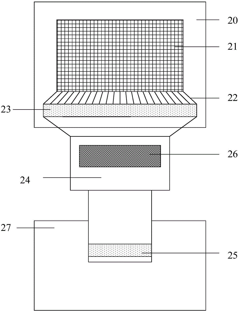
However, it is still impossible to improve the stretch limit on one side of the amorphous silicon glass panel 20—the problem that the readout lead 22 needs to be expanded, and the wiring on the flexible circuit board 24 will still be relatively long, which will introduce noise and have relatively large Parasitic capacitance
[0010] The common problem of the above two methods is that both need to use flexible circuit boards. It is necessary to bond the connector of the flexible circuit board to the substrate, and connect the other end of the flexible circuit board to the printed circuit board with the connector. These two processes They are more complicated, and it is easy to cause the problem of low yield rate.
In particular, the connection between the flexible circuit board and the substrate requires a large area, and a wide glue bonding area is required, which increases the area of ​​the substrate and the entire product

Method used


Image

  • Fingerprint sensor
  • Fingerprint sensor
  • Fingerprint sensor

Examples


Embodiment Construction

[0042] It can be seen from the background technology that how to effectively connect the readout circuit chip and the amorphous silicon TFT photosensitive panel, improve the signal-to-noise ratio, simplify the system complexity, and reduce the system size is a key issue.

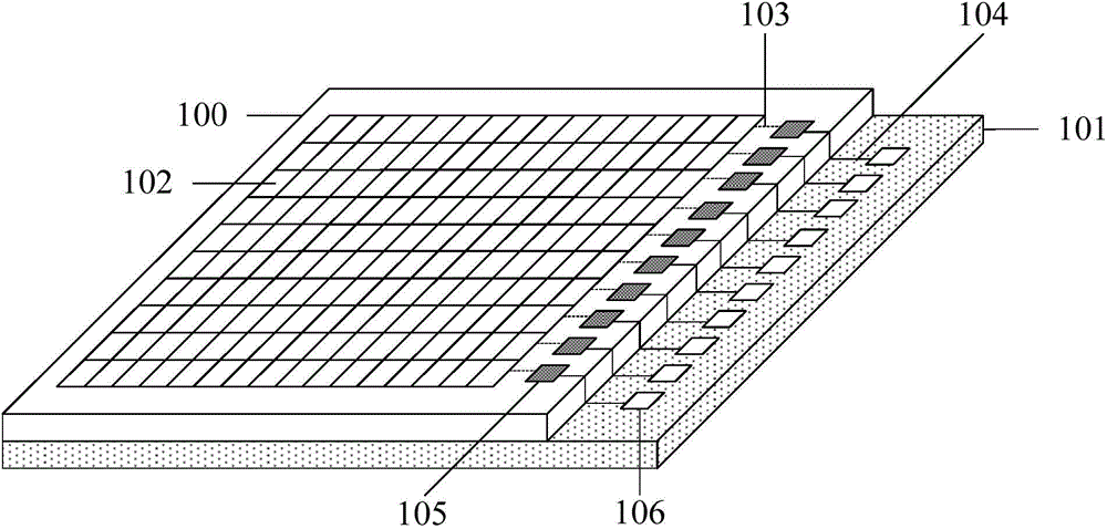
[0043] In order to solve the above technical problems, the present invention provides a fingerprint sensor, comprising:

[0044] Substrate;

[0045] Pixel units arranged in an array on the substrate are used to collect fingerprint signals;

[0046] The signal line on the substrate is used to transmit the fingerprint signal collected by the pixel unit;

[0047] A plurality of exposed substrate binding pads on the substrate are correspondingly connected to the signal lines;

[0048] A printed circuit board located under the substrate for connection to other systems;

[0049] Multiple exposed circuit board bond pads located on the printed circuit board;

[0050] The binding wires connecting the substrate bind...


PUM

PropertyMeasurementUnit
Sizeaaaaaaaaaa

Abstract

A fingerprint sensor comprises a substrate, pixel units, signal lines, multiple exposed substrate binding pads, a printed circuit board, multiple exposed circuit board binding pads and binding lines, wherein the pixel units are arranged on the substrate in an array mode for acquiring fingerprint signals; the signal lines are located on the substrate for transmitting the fingerprint signals acquired by the pixel units; the multiple exposed substrate binding pads are located on the substrate and are correspondingly connected with the signal lines; the printed circuit board is located below the substrate for being connected with other systems; the multiple exposed circuit board binding pads are located on the printed circuit board; and the binding lines are connected with the substrate binding pads and the circuit board binding pads for realizing electrical conduction between the substrate binding pads and the circuit board binding pads. Thus, the use of a flexible circuit board is saved; the signal line wiring length is shortened; noise of the device can be effectively reduced; the stability and the yield rate of the device are improved; the area and the volume occupied by the fingerprint sensor can be narrowed; and the device manufacturing cost is reduced.

Description

technical field [0001] The invention relates to the field of sensors, in particular to a fingerprint sensor. Background technique [0002] There are several types of fingerprint recognition sensors, such as optical, capacitive, and ultrasonic. Among them, the optical fingerprint sensor is mainly divided into focusing type and non-focusing type. [0003] The focused optical fingerprint sensor mainly uses the principle of refraction and reflection of light: put your finger on the optical lens, and the finger is illuminated by the built-in light source; the light is generated from the bottom of the device, refracted by the prism, and then emitted, and the emitted light is reflected on the surface of the finger. The angle of refraction on the uneven lines is different, and the light and shade of the reflected light are different, forming a spatial distribution image of light intensity; through the optical system, it is projected and focused on a charge-coupled device (CMOS devi...

Claims


Application Information

Patent Timeline
IPC IPC(8): G06K9/00G06K9/20
Inventor 林崴平朱虹
Owner SHANGHAI OXI TECH
Learn More