Device, method and system for detecting micro gap based on industrial equipment

A technology for industrial equipment and detection devices, which is applied in the field of micro-gap detection devices, can solve the problems of poor detection effect, detection of PCB boards or micro-gap products to be tested, insufficient range of application, poor practicability and adaptability, etc.

Inactive Publication Date: 2016-06-01
GUANGDONG ZHENGYE TECH
View PDF8 Cites 14 Cited by
  • Summary
  • Abstract
  • Description
  • Claims
  • Application Information

AI Technical Summary

Problems solved by technology

[0004] At present, the detection methods of PCB line width and the high-precision micro-gap of industrial equipment mainly include manual visual inspection, automatic X-ray inspection and automatic optical inspection, but they are limited by the refinement of the circuit, the diversification of factors affecting etching, Diversification of PCB boards or micro-gap products to be tested and the background environment lead to poor detection results. The types and scope of application of PCB boards or micro-gap products to be te

Method used


Image

  • Device, method and system for detecting micro gap based on industrial equipment
  • Device, method and system for detecting micro gap based on industrial equipment
  • Device, method and system for detecting micro gap based on industrial equipment

Examples


Embodiment Construction

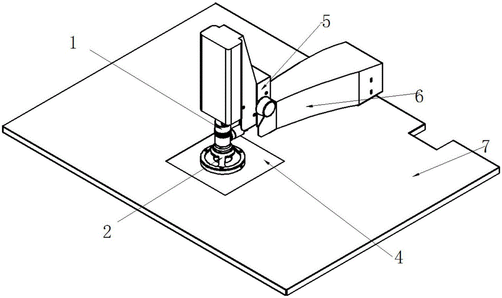
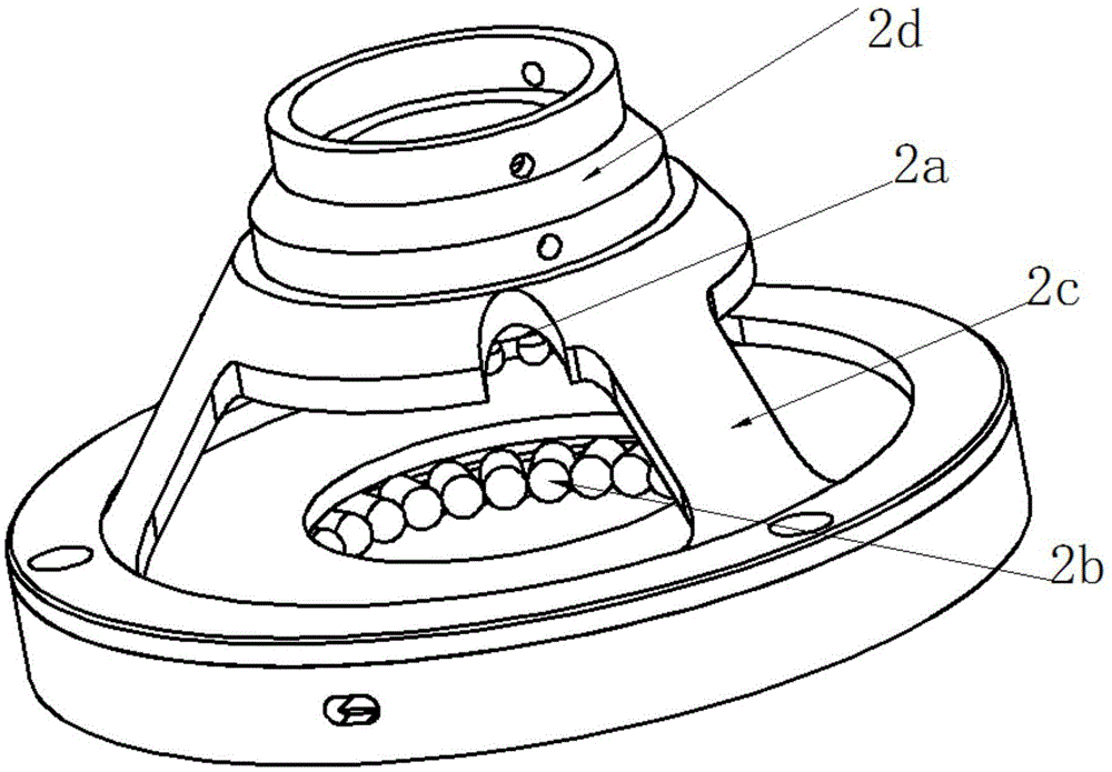
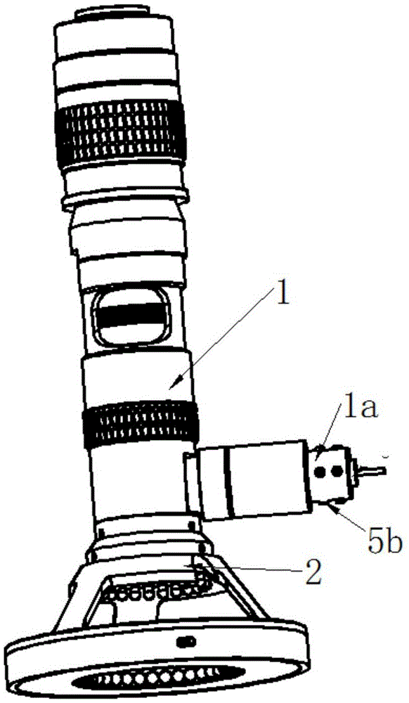
[0047] The embodiment of the present invention provides a micro-gap detection device, method and system based on industrial equipment. The lower end of the lens barrel is connected to the dual light source assembly through the lens barrel and the dual light source assembly. The dual light source assembly includes an upper annular light source assembly and a lower annular light source assembly. The light source component realizes the image processing of PCB boards or products under test with small gaps illuminated by different light sources, and performs subsequent detection of small gaps based on industrial equipment.

[0048]In order to make the purpose, features and advantages of the present invention more obvious and understandable, the technical solutions in the embodiments of the present invention will be clearly and completely described below in conjunction with the accompanying drawings in the embodiments of the present invention. Obviously, the following The described e...


PUM


Abstract

The embodiment of the invention discloses a device, a method and a system for detecting a micro gap based on industrial equipment. A lens tube and a duel-light source assembly are included; the lower end of the lens tube is connected with the duel-light source assembly; the duel-light source assembly comprises an upper annular light source assembly and a lower annular light source assembly; and thus, irradiation of different light sources is realized for image processing on a PCB or a micro gap to-be-detected product; and subsequent industrial equipment-based micro gap detection is carried out. The subsequent industrial equipment-based micro gap detection device comprises the lens tube and the duel-light source assembly; the lower end of the lens tube is connected with the duel-light source assembly; and the duel-light source assembly comprises the upper annular light source assembly and the lower annular light source assembly.

Description

technical field [0001] The invention relates to the technical field of quality detection of printed circuit boards, in particular to a micro gap detection device, method and system based on industrial equipment. Background technique [0002] With the continuous maturity of optical imaging equipment and the rapid development of computer vision technology, it has become an emerging development trend to use hardware equipment and software algorithms to freely match and combine in the field of PCB inspection to coordinate and complete efficient and high-quality inspection tasks. [0003] In view of the miniaturization and integration development trend of electronic product chips or the high-precision micro-gap of industrial equipment, the requirements for PCB are urgently reflected in the multi-layer and dense wiring of PCB. High-precision, thin wires, high density, and small spacing are developing in the direction of development, which leads to the fact that the characteristic ...

Claims


Application Information

Patent Timeline
IPC IPC(8): G01B11/14
CPCG01B11/14
Inventor 侯志松龙庆文周江秀敖荟兰陈伯平肖林锋张宇郑臣邓世文徐地华
Owner GUANGDONG ZHENGYE TECH
Why Eureka
Try Eureka