Chip offset detection device and method and chip burning method and system

A detection method and detection device technology, applied in the electronic field, can solve the problems of brightness, high position, high cost, prolonging the burning time, etc.

Inactive Publication Date: 2016-06-01
UNIVERSAL GLOBAL TECH KUNSHAN
View PDF3 Cites 2 Cited by
  • Summary
  • Abstract
  • Description
  • Claims
  • Application Information

AI Technical Summary

Problems solved by technology

However, using a CCD detector to detect blank chips is an optical method, which has extremely high environmenta

Method used


Image

  • Chip offset detection device and method and chip burning method and system
  • Chip offset detection device and method and chip burning method and system
  • Chip offset detection device and method and chip burning method and system

Examples


Embodiment Construction

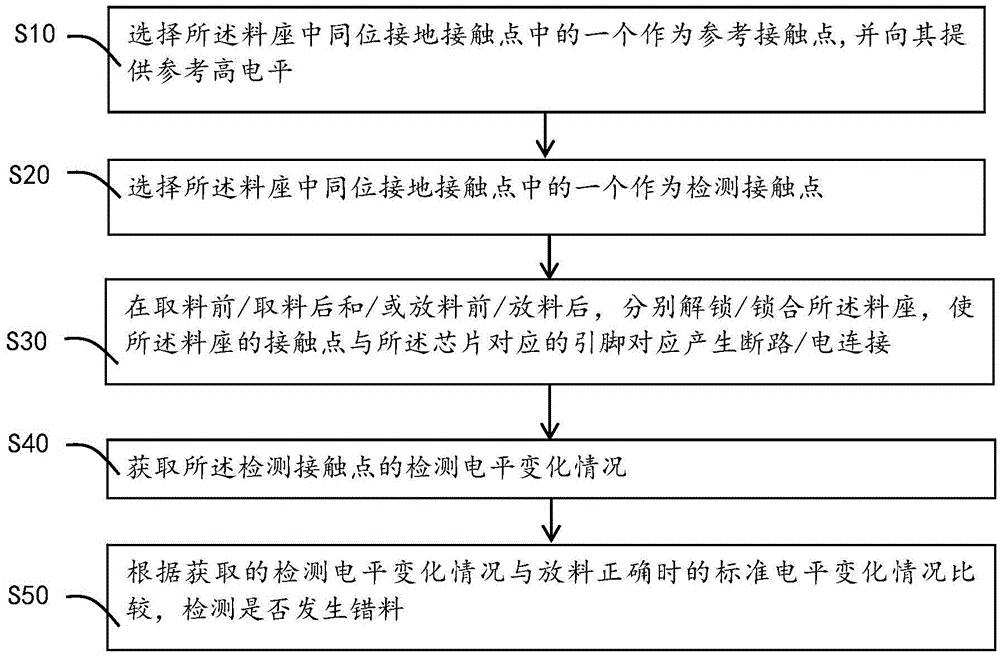
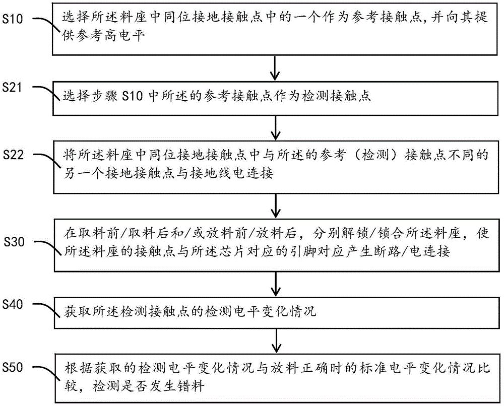
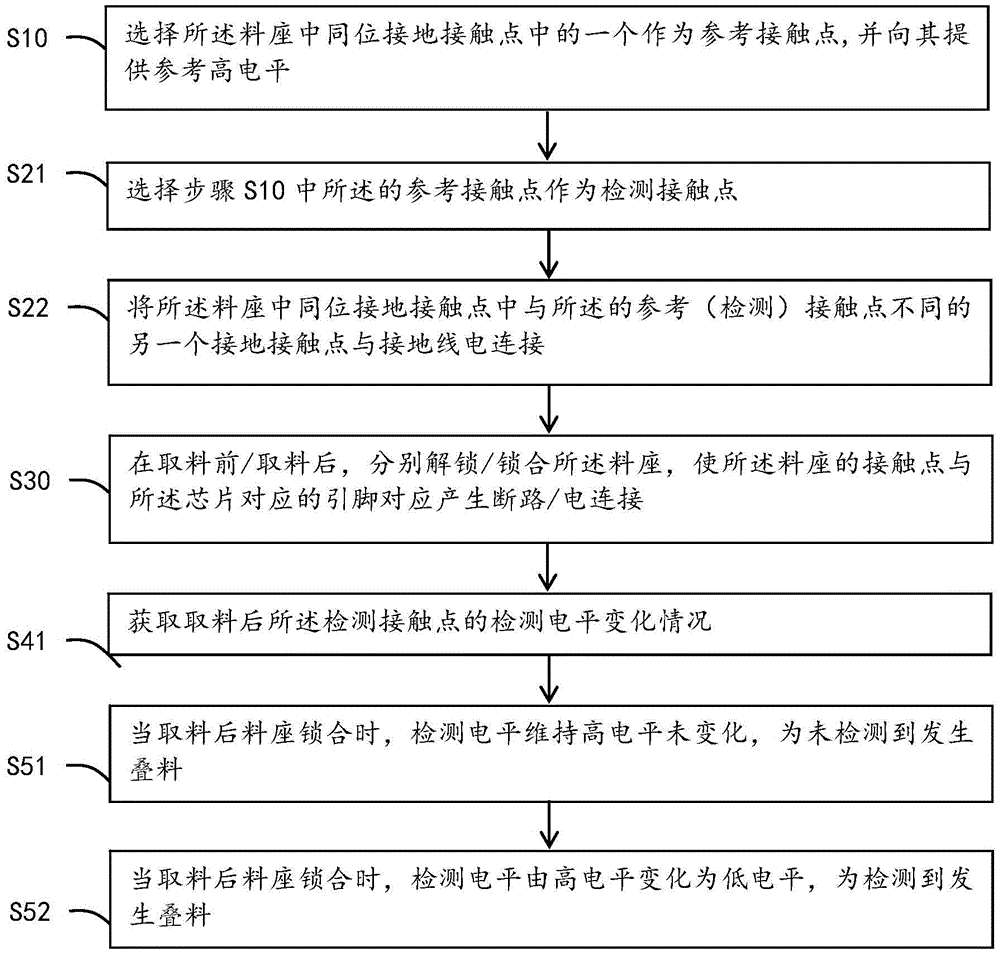
[0061] In order to more clearly illustrate the embodiments of the present invention or the technical solutions in the prior art, the specific implementation manners of the present invention will be described below with reference to the accompanying drawings. Obviously, the accompanying drawings in the following description are only some embodiments of the present invention, and those skilled in the art can obtain other accompanying drawings based on these drawings and obtain other implementations. In the present invention, for the convenience of expression, the steps are numbered, such as S10, S20, etc., but it does not mean that there must be a sequence relationship between the preceding and following steps.

[0062] Such as figure 1 It is a schematic flow chart of the first embodiment of the chip wrong material detection method in the present invention. According to this embodiment, a chip wrong material detection method is used to detect the chip discharged into the materi...


PUM


Abstract

The invention provides a chip offset detection device and method and a chip burning system and method. The offset detection method comprises the steps that one of grounding contact points at the same position in a material base is selected to serve as a reference contact point, and a reference high level is supplied to the reference contact point; one the grounding contact points at the same position in the material base is selected to serve as a detection contact point; the material base is unlocked/locked before/after material taking and/or before/after material discharging, the contact points of the material base are made to be in electrical correspondence with corresponding pins of a chip to form short-circuit/electrical connection; changes in the detection level of the detection contact point is obtained; the obtained changes in the detection level are compared with changes in a standard level at the time of correct discharging, and whether offset happens or not is detected. Whether offset or burning happens or not is judged according to the changes in the detection level of the detection contact point in the offset detection device, so that simplicity and convenience are achieved, and meanwhile burning time is saved.

Description

technical field [0001] The present invention relates to the field of electronic technology, in particular to a chip wrong material detection device and a wrong material detection method based on the wrong material detection device, and also relates to a chip burning method and a burning system thereof. Background technique [0002] Electrically Erasable Programmable Read-Only Memory (EEPROM) chip is an erasable programmable read-only memory chip that does not lose data after power failure, which can be erased on a computer or on a special device. With information, reprogramming, the method of use is plug and play. At present, many hardware needs to use EEPROM chip to store some key hardware data or configuration information, for example, the EEPROM chip of the network card of the mainboard of the computer, etc., the data stored inside is naturally different due to different functions. [0003] In the process of burning data into the EEPROM chip, first put the EEPROM chip ma...

Claims


Application Information

Patent Timeline
IPC IPC(8): G11C16/10G11C16/20G11C29/00G11C29/12
CPCG11C16/10G11C16/20G11C29/12G11C29/82G11C2029/4402
Inventor 任加华路晓东钱之政赵树磊刘上林大毅
Owner UNIVERSAL GLOBAL TECH KUNSHAN
Why Eureka
Try Eureka