

A LED chip structure with increased light-emitting area and manufacturing method
A technology of LED chip and light-emitting area, which is applied in the direction of semiconductor devices, electrical components, circuits, etc., can solve the problems of loss of light-emitting area and further improvement of luminous efficiency, and achieve the effect of chip voltage optimization
- Summary
- Abstract
- Description
- Claims
- Application Information
AI Technical Summary
Problems solved by technology
Method used
Image

Examples
Embodiment Construction
[0046] The present invention will be described in detail below in conjunction with the accompanying drawings and specific embodiments.
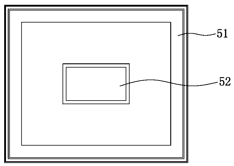
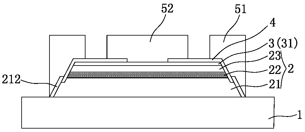
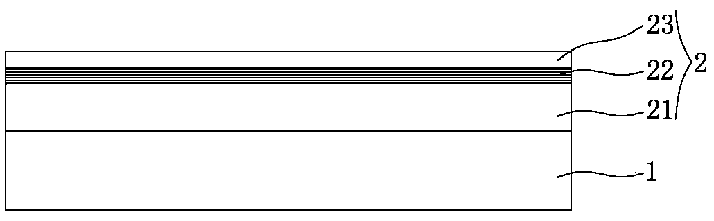
[0047] refer to Figures 1 to 3f As shown, Embodiment 1 of an LED chip structure with increased light-emitting area disclosed in the present invention includes a substrate 1 , an epitaxial layer 2 , a conductive layer 3 , an insulating layer 4 , an N electrode 51 and a P electrode 52 .
[0048] The epitaxial layer 2 is composed of N-GaN 21 , active light emitting layer 22 and P-GaN 23 which are sequentially formed, and the N-GaN 21 is formed on the substrate 1 . The conductive layer 3 is formed on the P-GaN 23, and the P electrode 52 is formed on the conductive layer 3; in this embodiment, the conductive layer 3 is a metal reflective layer 31, forming a flip chip. The metal reflective layer 31 is made of silver, titanium, aluminum, chromium, indium, tin, gold and alloys thereof, and is arranged in a single-layer or multi-layer structure.
...
PUM
 Abstract
Description
Claims
Application Information