

Storage device
A storage device and storage unit technology, applied in the field of electronics, can solve problems such as reducing the transmission rate of transmission lines, and achieve the effect of ensuring impedance consistency and transmission rate
- Summary
- Abstract
- Description
- Claims
- Application Information
AI Technical Summary
Problems solved by technology
Method used
Image

Examples
Embodiment 1
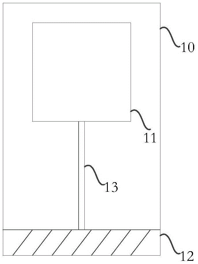
[0046] Please refer to figure 1 , is a schematic structural diagram of a storage device according to a first preferred embodiment of the present application. The storage device is described in detail below.
[0047] A storage device comprising:
[0048] a first circuit board 10;
[0049] a storage unit 11 arranged on the first circuit board 10;
[0050] A connection structure 12, arranged on the first circuit board 10;
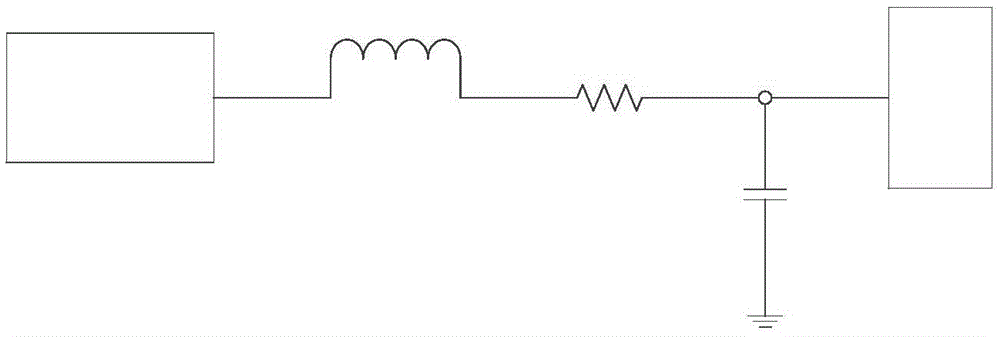
[0051] a transmission line 13, arranged between the storage unit 11 and the connection structure 12;
[0052] Wherein, the transmission line 13 is provided with an inductance element and a resistance element connected in series with the inductance element for adjusting the impedance of the transmission line 13 so as to maximize the transmission rate of the transmission line 13 .
[0053]The storage device in the embodiment of the present application can be designed as a U disk, through the connection structure 12 and other electronic equipment, such as: a...
PUM
 Abstract
Description
Claims
Application Information