Flicker debugging method and device for liquid crystal display television

A technology of liquid crystal TV and debugging method, which is applied to the parts of color TV, parts of TV system, TV, etc., can solve the problems such as no longer applicable, and achieve the effect of saving cost and improving production efficiency

Active Publication Date: 2016-06-15
SICHUAN CHANGHONG ELECTRIC CO LTD
View PDF3 Cites 18 Cited by
  • Summary
  • Abstract
  • Description
  • Claims
  • Application Information

AI Technical Summary

Problems solved by technology

[0002] In the field of LCD TV, with the development of integrated chip technology, the TV logic signal control board has the ability to be integrated into the TV core. After the TV core is installed, the i

Method used


Image

  • Flicker debugging method and device for liquid crystal display television
  • Flicker debugging method and device for liquid crystal display television

Examples


Embodiment 1

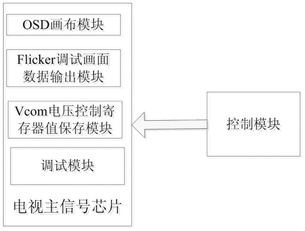
[0030] figure 1 It is a schematic structural diagram of a Flicker debugging device for an LCD TV provided in Embodiment 1 of the present invention. Such as figure 1 As shown, the device includes a TV main signal chip and a control module, and the TV main signal chip includes an OSD canvas module, a Flicker debugging screen data output module, a Vcom voltage control register value storage module and a debugging module.

[0031] The OSD canvas module is configured to: generate Flicker debugging screen data, the debugging screen data includes a test picture, a Vcom voltage value progress bar, and the Vcom voltage value is the current value of the Vcom voltage control register corresponding to the P-Gamma chip.

[0032] The Flicker debugging screen data output module is configured to: output the Flicker debugging screen data to an LCD TV screen for display.

[0033] The Vcom voltage control register value storage module is configured to: when the middle part of the test picture ...

Embodiment 2

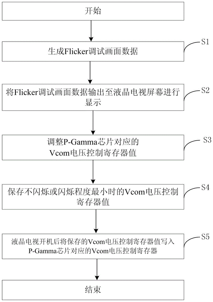
[0038] figure 2 It is a flow chart of the Flicker debugging method of the LCD TV provided by Embodiment 2 of the present invention. Such as figure 2 As shown, steps S1 to S5 are included, and the above steps will be described in detail below.

[0039] Step S1: Generate Flicker debugging screen data.

[0040] In step S1, the OSD canvas module in the TV main signal chip generates Flicker debugging picture data, wherein the debugging picture data includes a test picture, Vcom (VoltageofCommonelectrode, common electrode voltage) voltage value progress bar, and the Vcom voltage value is corresponding to the P-Gamma chip Current value of the Vcom voltage control register. It should be noted that the test picture is designed according to the requirements of the LCD screen, and the point-to-point format display of the test picture needs to be realized through the OSD canvas module.

[0041] Step S2: output the Flicker debugging screen data to the LCD TV screen for display.

[0...


PUM


Abstract

The invention relates to the technical field of liquid crystal display televisions, provides a Flicker debugging method and device for a liquid crystal display television, and aims to solve the problem that an existing Flicker debugging method for liquid crystal screens is not suitable for new on-screen signals any more. The device comprises a television main signal chip and a control module, wherein the television main signal chip comprises an OSD (On Screen Display) canvas module, a Flicker debugging picture data output module, a Vcom (Voltage of Common electrode) voltage control register value saving module and a debugging module. According to the technical scheme provided by the invention, the problem of incapability of implementing function debugging through existing debugging equipment due to change of an on-screen signal interface is solved. Meanwhile, corresponding debugging equipment such as a signal generator, a color analyzer and a computer are saved; the cost is saved; and the production efficiency of the liquid crystal display television is increased.

Description

technical field [0001] The invention relates to the technical field of liquid crystal televisions, in particular to a Flicker debugging method and device for liquid crystal televisions. Background technique [0002] In the field of LCD TV, with the development of integrated chip technology, the TV logic signal control board has the ability to be integrated into the TV core. After the TV core is installed, the interface of the upper screen signal will become a mini-LVDS signal interface. Due to the change of the signal interface, the current Flicker debugging method for the screen glass will no longer be applicable. Contents of the invention [0003] 【Technical problems to be solved】 [0004] The purpose of the present invention is to provide a Flicker debugging method and device for LCD TVs, so as to solve the problem that the current Flicker debugging method for LCD screens is no longer applicable to new screen-up signals. [0005] 【Technical solutions】 [0006] The pr...

Claims


Application Information

Patent Timeline
IPC IPC(8): H04N5/44H04N17/00
CPCH04N17/004H04N21/42204H04N2017/008
Inventor 朱大林王承健胥成祥张博
Owner SICHUAN CHANGHONG ELECTRIC CO LTD
Why Eureka
Try Eureka