Laser beam machining apparatus and wafer processing method

A laser processing and laser technology, applied in laser welding equipment, metal processing equipment, manufacturing tools, etc., can solve the problems of increased process, device damage, poor productivity, etc., and achieve the effect of solving device damage

Active Publication Date: 2016-06-22
DISCO CORP
View PDF9 Cites 9 Cited by
  • Summary
  • Abstract
  • Description
  • Claims
  • Application Information

AI Technical Summary

Problems solved by technology

[0004] However, in order to position the converging point of the laser light inside the wafer, a spot such as the bottom surface of the cone must be positioned on the surface to be irradiated which is the front side of the planned dividing line formed on the wafer. If the width of the planned division line is large, the spot of the laser light will exceed the planned division line and be positioned on the device, and the device will be damaged.
[0008] However, if a laser processing method is implemented in which the laser light is irradiated from the back side of the wafer by positioning the laser beam's converging point inside and irradiating the laser light along the planned dividing line, the wafer needs to be reversed in the subsequent processing steps, and there is an increase in the production process. issues like sex difference

Method used


Image

  • Laser beam machining apparatus and wafer processing method
  • Laser beam machining apparatus and wafer processing method
  • Laser beam machining apparatus and wafer processing method

Examples


Embodiment Construction

[0032] Hereinafter, preferred embodiments of the laser processing apparatus and the wafer processing method according to the present invention will be described in detail with reference to the drawings.

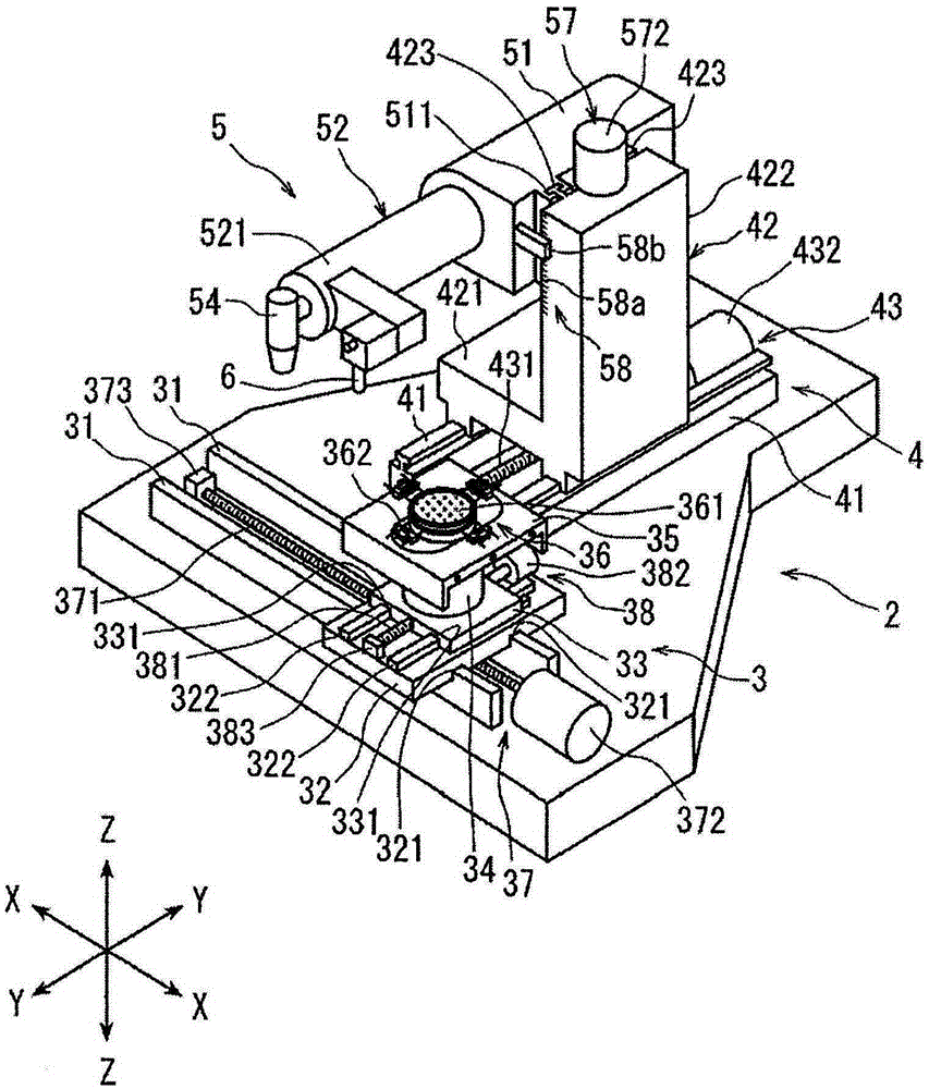
[0033] figure 1 is a perspective view of a laser processing device for implementing the laser spot shape detection method of the present invention. figure 1 The laser processing apparatus shown has: a stationary base 2; a chuck table mechanism 3 for holding a workpiece, which is arranged on the substrate so as to be movable in the processing feed direction (X-axis direction) indicated by arrow X. This stationary base 2; a laser beam irradiation unit support mechanism 4 arranged on the stationary base so as to be movable in an index feed direction (Y-axis direction) indicated by an arrow Y perpendicular to the above-mentioned X-axis direction. 2; and a laser beam irradiation unit 5, which is arranged on the laser beam in a manner capable of moving in a focus point position ad...


PUM


Abstract

A laser beam machining apparatus and a wafer processing method. The laser beam machining apparatus comprises: a to-be-processed object maintaining means having a maintaining surface for maintaining a to-be-processed object; a laser beam irradiation means for irradiating laser beams to the to-be-processed object which is maintained on the to-be-processed object maintaining means; a moving means for enabling the to-be-processed object maintaining means and the laser beam irradiation means to relatively move; and a shooting means for shooting a to-be-processed area of the to-be-processed object which is maintained on the to-be-processed object maintaining means. The laser beam irradiation means comprises: a laser beam oscillating means for oscillating the laser beams; a condenser for converging the laser beams oscillated from the laser beam oscillating means and irradiating the to-be-processed object which is maintained on the to-be-processed object maintaining means; and a spot adjusting means arranged between the laser beam oscillating means and the condenser to perform adjustment to make a spot of the laser beams irradiated on the to-be-processed object which is maintained on the to-be-processed object maintaining means to be a spot having a suitable size on an irradiated surface of the to-be-processed object.

Description

technical field [0001] The present invention relates to a laser processing device and a wafer processing method, wherein a modified layer is formed along a planned division line inside a wafer such as a semiconductor wafer. Background technique [0002] In the manufacturing process of semiconductor devices, a plurality of regions are divided by dividing lines arranged in a grid on the front surface of a substantially disk-shaped semiconductor wafer, and devices such as ICs and LSIs are formed in the divided regions. Then, individual semiconductor devices are manufactured by cutting the semiconductor wafer along planned dividing lines to divide regions where the devices are formed. [0003] As a method of dividing the above-mentioned wafer, a laser processing method has been attempted in which a pulsed laser beam of a wavelength transparent to the wafer is used, and the focused point is aligned with the inside of the region to be divided, and the pulsed laser beam is irradiat...

Claims


Application Information

Patent Timeline
IPC IPC(8): B23K26/03B23K26/0622
CPCB23K26/03
Inventor 古田健次汤平泰吉
Owner DISCO CORP
Why Eureka
Try Eureka