Array substrate, manufacturing method thereof, and display device

A technology of an array substrate and a manufacturing method, which is applied in the field of display and can solve problems such as poor display

Active Publication Date: 2018-09-04
BOE TECH GRP CO LTD +1
View PDF4 Cites 0 Cited by
  • Summary
  • Abstract
  • Description
  • Claims
  • Application Information

AI Technical Summary

Problems solved by technology

[0004] Aiming at the defects of the prior art, the present invention provides an array substrate and its manufacturing method, and a display device, which can solve the problem that the via holes in the GOA region are easily connected to the ITO electrode layer on the side of the color filter substrate in the prior art, resulting in poor display The problem

Method used


Image

  • Array substrate, manufacturing method thereof, and display device
  • Array substrate, manufacturing method thereof, and display device
  • Array substrate, manufacturing method thereof, and display device

Examples


Embodiment Construction

[0055] The following will clearly and completely describe the technical solutions in the embodiments of the present invention with reference to the accompanying drawings in the embodiments of the present invention. Obviously, the described embodiments are only some, not all, embodiments of the present invention. Based on the embodiments of the present invention, all other embodiments obtained by persons of ordinary skill in the art without making creative efforts belong to the protection scope of the present invention.

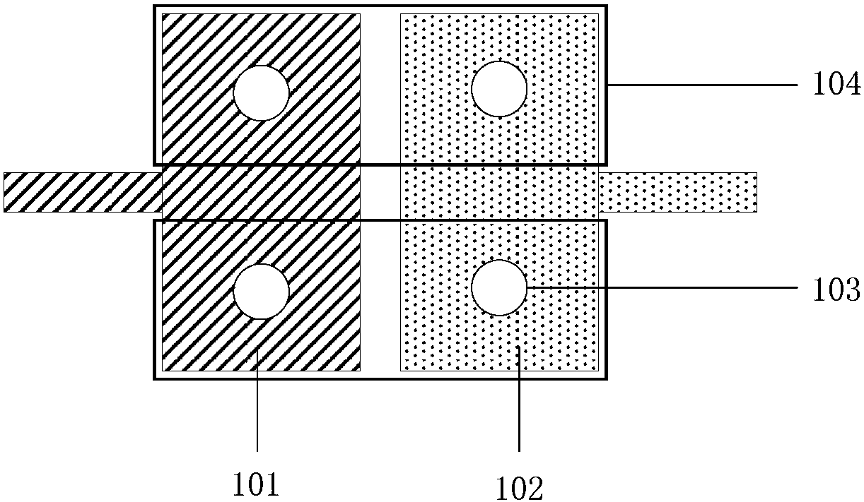
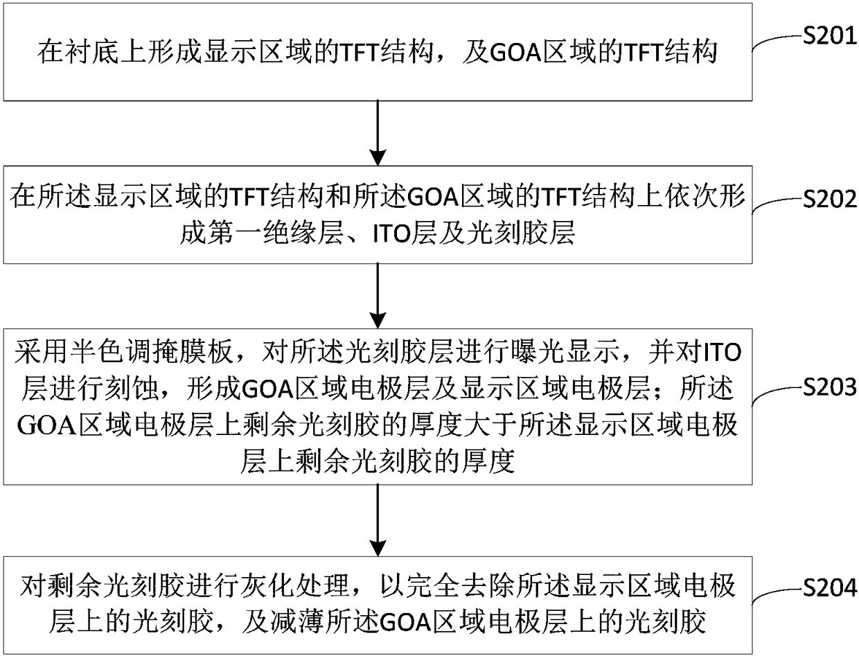
[0056] figure 2 It is a schematic flowchart of a manufacturing method of an array substrate provided by an embodiment of the present invention. The array substrate in this embodiment includes a display area and a GOA area. Such as figure 2 As shown, the manufacturing method of the array substrate in this embodiment specifically includes the following steps:

[0057] S201: Forming a thin film transistor TFT structure in a display region and a TFT structure ...


PUM


Abstract

The invention provides an array substrate, a manufacturing method thereof, and a display device. Wherein, the method includes: forming the TFT structure of the display region and the TFT structure of the GOA region on the substrate; sequentially forming a first insulating layer, an ITO layer and a photoresist layer on the TFT structure; using a half-tone mask , exposing and developing the photoresist layer, and etching the ITO layer to form a GOA region electrode layer and a display region electrode layer; the thickness of the remaining photoresist on the GOA region electrode layer is greater than that of the display region The thickness of the remaining photoresist on the regional electrode layer; ashing the remaining photoresist to completely remove the photoresist on the display region electrode layer and thin the photoresist on the GOA region electrode layer . In the embodiment of the present invention, the photoresist can protect the via holes in the GOA region, thereby making it possible to further reduce the frame of the panel to form a TN type narrow frame display panel.

Description

technical field [0001] The present invention relates to the field of display technology, in particular to an array substrate, a manufacturing method thereof, and a display device. Background technique [0002] With the technical development of thin film transistor-liquid crystal display (TFT-LCD for short), especially small-sized screens have higher and higher requirements for narrow borders, the gate drive on array (Gate Drive On Array, GOA for short) technology is used more frequently. GOA technology can integrate the gate drive circuit on the TFT substrate, reduce the use of Gate IC, and reduce the frame design of the panel, making the panel more in line with the development trend of technology. [0003] In the design process of the TN display panel, due to the characteristics of its liquid crystal deflection principle, it is necessary to conduct the ITO electrode layer on the color filter substrate side with the pixel electrode on the array substrate side by using the g...

Claims


Application Information

Patent Timeline
Patent Type & Authority Patents(China)
IPC IPC(8): H01L27/12H01L21/77
CPCH01L27/1248H01L27/1288G02F1/13454G09G2300/0408G02F1/136236H01L27/1225H01L27/124H01L27/1292G02F1/1368H01L21/12H01L21/77H01L23/552H01L27/12
Inventor 卢彦春蒋学兵
Owner BOE TECH GRP CO LTD
Why Eureka
Try Eureka