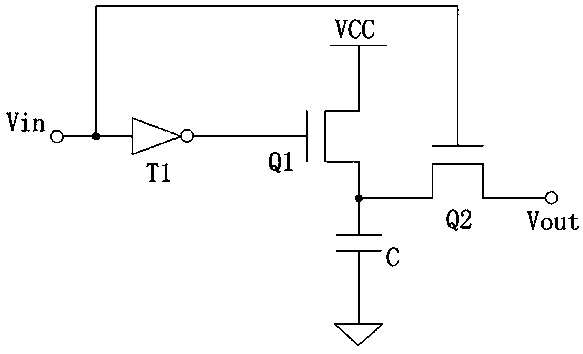
Voltage output trimming circuit
A technology of fine-tuning circuit and voltage output, which is applied in the direction of conversion equipment without intermediate conversion to AC, can solve the problems of low precision, adjustable resistance heating, increase the workload of engineers, etc., to achieve simple circuit structure, high fine-tuning precision, and implementation low cost effect
- Summary
- Abstract
- Description
- Claims
- Application Information
AI Technical Summary
Problems solved by technology
Method used
Image
Examples
Embodiment Construction
[0009] Attached as follows figure 1 , to further describe the application scheme:
[0010] A voltage output fine-tuning circuit, including MOS transistors Q1, Q2, capacitor C, and inverter T1, the MOS transistor Q1, capacitor C are connected in series between the power supply VCC terminal and the ground terminal, and its gate is passed through the inverter The phase device T1 is connected to the input terminal Vin of the circuit, and the MOS transistor Q1 is used to realize on-off according to the inverting signal of the input terminal Vin, and to charge the capacitor C; the MOS transistor Q2 is connected to the capacitor C and the output terminal Vout of the circuit, Its gate is connected to the input terminal Vin of the circuit, and is used for switching on and off according to the signal of the input terminal Vin, and outputting the electric quantity in the capacitor C.
[0011] The MOS transistors Q1 and Q2 are both PMOS transistors or NMOS transistors.
[0012] The inpu...
PUM
 Abstract
Description
Claims
Application Information
