Monolithic integration method of hyperspectral image sensor

A hyperspectral image and image sensor technology, applied in the field of monolithic integration of hyperspectral image sensors, can solve the problems of poor step structure height uniformity, device failure, etc., achieve easy etching, reduce device failure rate, and improve product yield Effect

Active Publication Date: 2016-07-06
INST OF MICROELECTRONICS CHINESE ACAD OF SCI
View PDF4 Cites 8 Cited by
  • Summary
  • Abstract
  • Description
  • Claims
  • Application Information

AI Technical Summary

Problems solved by technology

[0008] In order to solve the problem of poor step structure height uniformity and device failure caused by the etching process, and to expand the selection range of materials used to make the transparent cavity layer, the invention provides a monolithic integrated hyperspectral image sensor method

Method used


Image

  • Monolithic integration method of hyperspectral image sensor
  • Monolithic integration method of hyperspectral image sensor
  • Monolithic integration method of hyperspectral image sensor

Examples


preparation example Construction

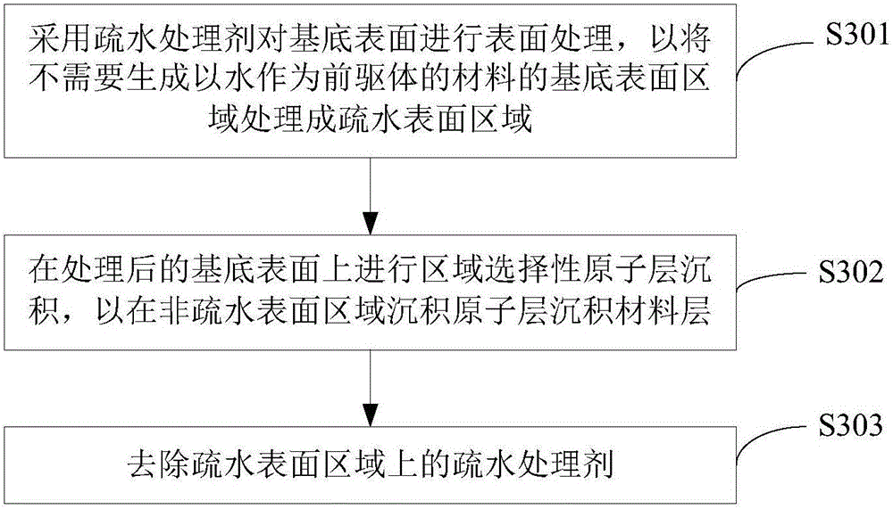
[0091] Figure 9 It is a schematic flowchart of a monolithic integration method of a hyperspectral image sensor provided by an embodiment of the present invention. Such as Figure 9 Shown, this preparation method comprises the following steps:

[0092] S901, pretreating the surface of the photosensitive region of the CMOS image sensor wafer to make it planar;

[0093] The schematic diagram of the cross-sectional structure corresponding to the process is shown in Figure 10A shown. This step is specifically as follows: the entire CMOS image sensor 101 wafer (including the surface of the photosensitive area 102 ) may be planarized by using a chemical mechanical polishing (CMP) process to make the surface of the photosensitive area flat.

[0094] S902, forming a bottom reflective layer on the surface of the photosensitive region of the preprocessed CMOS image sensor wafer:

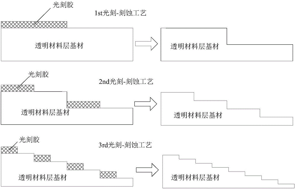
[0095] Figure 10B It is a schematic cross-sectional view of the structure corresponding to this pro...

Embodiment approach

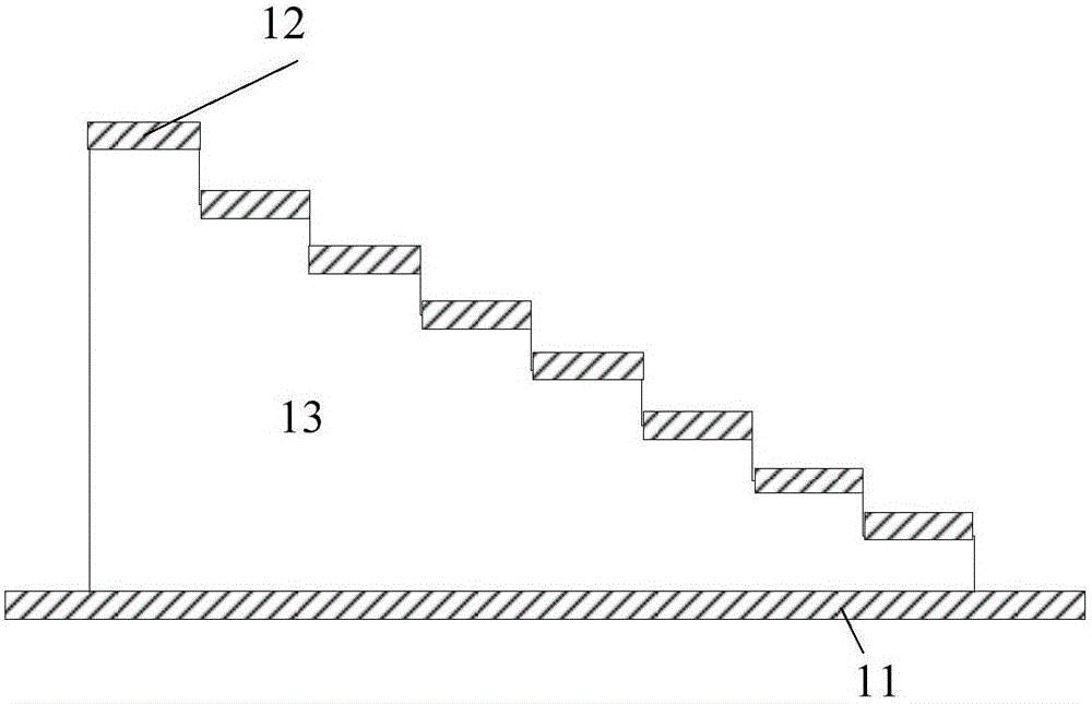
[0179] Through the first and second specific implementation manners of step S903 , the purpose of forming N step structures on the bottom reflective layer can be achieved through a relatively small number of area-selective atomic layer deposition processes. It should be noted that, in the embodiment of the present invention, step S903 is not limited to the above two specific implementation manners. For example, the present invention can also use each region-selective atomic layer deposition process to form a stepped structure, but this implementation method will The use of a large number of regional selective atomic layer deposition processes and the production of corresponding photoresist plates result in relatively high costs, increased errors, and very low efficiency.

[0180] It should be noted that the first specific implementation manner and the second specific implementation manner of the above-mentioned step S903 are examples of specific implementation manners for prepa...


PUM


Abstract

The invention discloses a monolithic integration method of a hyperspectral image sensor. The monolithic integration method comprises the following steps of forming a bottom reflection layer on the surface of a light sensing region of a complementary metal-oxide-semiconductor (CMOS) image sensor; forming a transparent cavity layer on the bottom reflection layer by an area selective atomic layer deposition process, wherein the transparent cavity layer comprise N step structures, N is equal to 2m, m is more than or equal to 1 and is an integer; and forming a top reflection layer on the transparent cavity layer. With the monolithic integration method of the hypersepctral image sensor, provided by the invention, the problem of non-uniform accumulation caused by an etching process adopted by the prior art is optimized, and meanwhile, the fact that the material of the cavity layer cannot be fabricated by the etching method is expanded on selection of the material of the cavity layer; the similar one-dimensional area selective atomic layer deposition mode can be extended, for example, another dimension is additionally arranged, several repeated regions are fabricated, and then a mosaic-type multiple cavity layers with different heights and the repeated structure can be formed; and the monolithic integration method can be applied to a snapshot hyperspectral image sensor, and the performance such as pixel of the hyperspectral image sensor is greatly improved.

Description

technical field [0001] The invention relates to the technical field of hyperspectral imaging, in particular to a single-chip integration method of a hyperspectral image sensor. Background technique [0002] Hyperspectral imaging technology can divide a composite spectrum into spectral bands of multiple wavelengths, which can achieve accurate analysis of sub-spectral segments. Therefore, hyperspectral imaging technology is widely used in remote sensing detection, food safety monitoring, and biomedical technology. Because the previous hyperspectral imaging system was based on laboratory research and development, there were problems such as large volume, slow analysis speed, and high cost. To solve the above problems, a research institute represented by the European Microelectronics Center (IMEC) proposes a method of monolithically integrating a filter in a CMOS image sensor. [0003] At present, a preparation method for the preparation of hyperspectral image sensors is to int...

Claims


Application Information

Patent Timeline
Patent Type & Authority Applications(China)
IPC IPC(8): H01L27/146H01L21/82
CPCH01L27/14685H01L27/14621H01L27/14625H01L27/14629H01L27/14632H01L27/14687H01L31/02162H01L31/02327H01L27/146H01L21/82
Inventor 崔虎山项金娟贺晓彬杨涛李俊峰赵超
Owner INST OF MICROELECTRONICS CHINESE ACAD OF SCI
Why Eureka
Try Eureka