Light emitting diode chip and manufacturing method therefor

A technology for light-emitting diodes and a manufacturing method, which is applied to electrical components, circuits, semiconductor devices, etc., can solve the problems of low reflectivity of non-vertically incident light and low luminous efficiency of LED chips, and achieves improved stability, improved luminous brightness and luminous The effect of efficiency

Active Publication Date: 2016-07-06
HC SEMITEK CORP
View PDF8 Cites 10 Cited by
  • Summary
  • Abstract
  • Description
  • Claims
  • Application Information

AI Technical Summary

Problems solved by technology

[0006] In order to solve the problem of low reflectance of DBR for non-perpendicularly incident light in the prior art, resulting in low luminous efficiency of LED chips, an embodiment of the present invention provides a light emitting diode chip and a manufacturing method thereof

Method used


Image

  • Light emitting diode chip and manufacturing method therefor
  • Light emitting diode chip and manufacturing method therefor
  • Light emitting diode chip and manufacturing method therefor

Examples


Embodiment 1

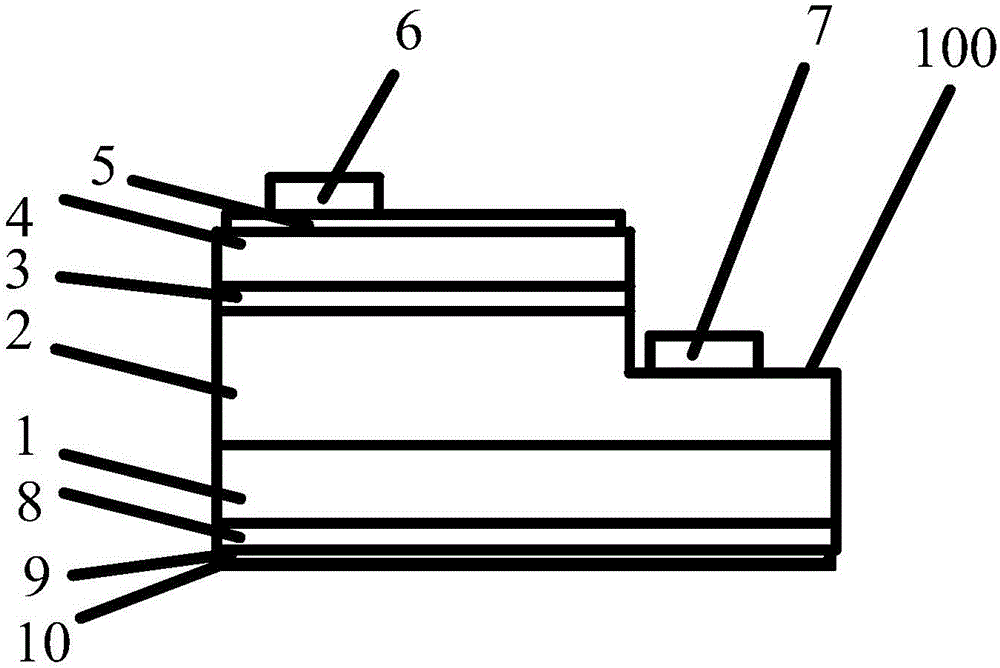
[0036] An embodiment of the present invention provides a light emitting diode chip, see figure 1 The light-emitting diode chip includes a substrate 1, an N-type layer 2, a light-emitting layer 3, a P-type layer 4, a transparent conductive film (TCO) 5, a P-type electrode 6, an N-type electrode 7, a DBR8, an Ag metal reflective layer 9 and The metal protection layer 10, the N-type layer 2, the light-emitting layer 3, and the P-type layer 4 are sequentially stacked on the first surface of the substrate 1, and the P-type layer 4 is provided with a groove extending from the P-type layer 4 to the N-type layer 2 100, the transparent conductive film 5 and the P-type electrode 6 are sequentially arranged on the P-type layer 4, the N-type electrode 7 is arranged on the N-type layer 2, and the DBR8, the Ag metal reflective layer 9, and the metal protective layer 10 are sequentially arranged on the substrate 1 The metal protective layer 10 and the DBR8 form a sealed space, the Ag metal r...

Embodiment 2

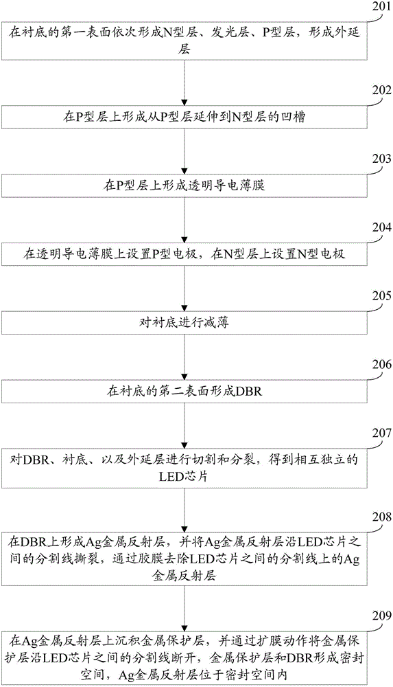
[0048] An embodiment of the present invention provides a method for manufacturing a light emitting diode chip, see figure 2 , the production method includes:

[0049] Step 201: sequentially forming an N-type layer, a light-emitting layer, and a P-type layer on the first surface of the substrate to form an epitaxial layer.

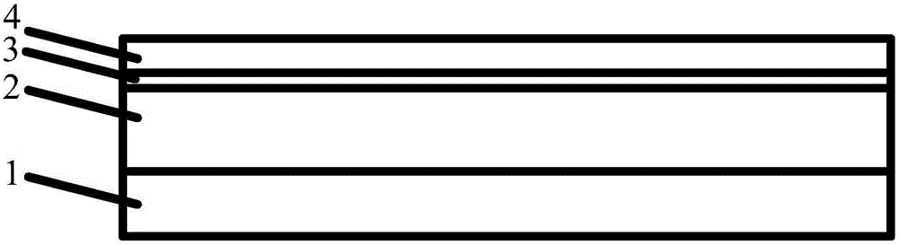
[0050] Figure 3a It is a schematic structural diagram of the LED chip after step 201 is performed. Wherein, 1 is a substrate, 2 is an N-type layer, 3 is a light-emitting layer, and 4 is a P-type layer.

[0051]In this embodiment, the N-type layer may be an N-type GaN layer, the light emitting layer may be alternately stacked InGaN layers and GaN layers, and the P-type layer may be a P-type GaN layer.

[0052] Optionally, the substrate can be one of a flat-surfaced sapphire substrate, a patterned sapphire substrate (Patterned Sapphire Substrate, PSS for short), a Si substrate, a GaN substrate, a SiN substrate, a SiC substrate, and a glass substrate. , ...


PUM


Abstract

The invention discloses a light emitting diode chip and a manufacturing method therefor, and belongs to the technical field of a semiconductor. The light emitting diode chip comprises a substrate, an N type layer, a light emitting layer, a P type layer, a transparent conductive thin film, a P type electrode, an N type electrode and a DBR, wherein the N type layer, the light emitting layer and the P type layer are laminated on the first surface of the substrate in sequence; a groove which extends from the P type layer to the N type layer is formed in the P type layer; the transparent conductive thin film and the P type electrode are arranged on the P type layer in sequence; the N type electrode is arranged on the N type layer; the DBR is arranged on the second surface of the substrate; the second surface refers to a surface opposite to the first surface; the light emitting diode chip also comprises an Ag metal reflective layer and a metal protection layer which are laminated on the DBR in sequence; a sealed space is formed by the metal protection layer and the DBR; and the Ag metal reflective layer is positioned in the sealed space. The light emitting diode chip can realize all-dimensional reflection, and meanwhile, the luminance and light emitting efficiency of the light emitting diode are improved.

Description

technical field [0001] The invention relates to the technical field of semiconductors, in particular to a light emitting diode chip and a manufacturing method thereof. Background technique [0002] Light Emitting Diode (LED for short) is a semiconductor diode that can convert electrical energy into light energy. [0003] The existing LED chip includes an N-type layer, a light-emitting layer, and a P-type layer stacked on the first surface of the substrate in sequence, and the P-type layer is provided with a groove extending from the P-type layer to the N-type layer, a transparent conductive film and The P-type electrodes are sequentially disposed on the P-type layer, the N-type electrodes are disposed on the N-type layer, and the second surface of the substrate is provided with a Distributed Bragg Reflection (Distributed Bragg Reflection, DBR for short). Wherein, the second surface is the surface opposite to the first surface. [0004] In the process of realizing the prese...

Claims


Application Information

Patent Timeline
Patent Type & Authority Applications(China)
IPC IPC(8): H01L33/46H01L33/00
CPCH01L33/005H01L33/46
Inventor 尹灵峰王江波
Owner HC SEMITEK CORP
Why Eureka
Try Eureka