
Light emitting diode encapsulating structure and manufacturing method thereof

A technology of light-emitting diodes and packaging structures, applied in the direction of electrical components, circuits, semiconductor devices, etc., can solve the problems of complex overall structure, heavy workload, unfavorable mass production, etc., and achieve the effects of improving efficiency, simple packaging structure, and cost saving

Inactive Publication Date: 2016-07-06
上海光纳电子科技有限公司
View PDF4 Cites 0 Cited by
  • Summary
  • Abstract
  • Description
  • Claims
  • Application Information

AI Technical Summary

Problems solved by technology

However, in the above two methods, the former needs to change the installation position of the light-emitting diode chip, so that the circuit connection and spatial position arrangement inside the lighting device need to be redesigned, and the latter needs to be achieved by adding an additional reflective structure. It is necessary to adjust the internal structure of the lighting device, which makes the overall structure complex, the workload is large, and it is not conducive to mass production

Method used


Image

  • Light emitting diode encapsulating structure and manufacturing method thereof
  • Light emitting diode encapsulating structure and manufacturing method thereof
  • Light emitting diode encapsulating structure and manufacturing method thereof

Examples


Embodiment Construction

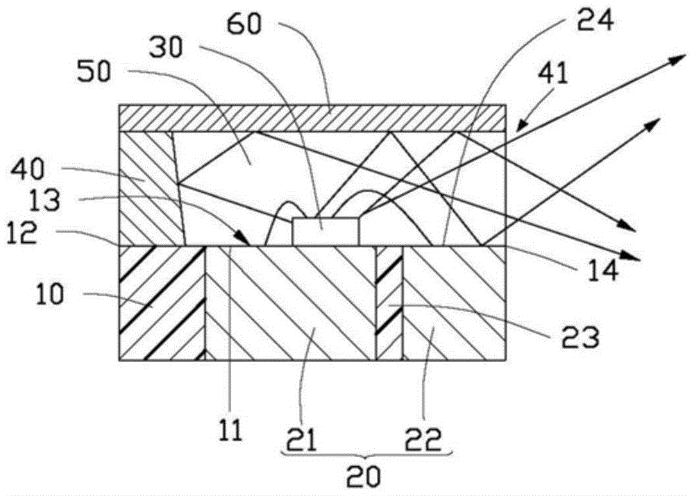
[0034] See figure 1 The light emitting diode packaging structure 100 provided by the embodiment of the present invention includes a substrate 10, two electrodes 20 arranged at intervals on the substrate 10, a light emitting diode chip 30 fixed on the first substrate 10 and electrically connected to the electrodes 20, located at The reflective cup 40 on the side of the LED chip 30 , the packaging layer 50 covering the LED chip 30 and a reflective layer 60 .

[0035] The substrate 10 is roughly in the shape of a rectangular plate, which includes four sides, a first side 11, a second side 12, a third side 13 and a fourth side 14, wherein the first side 11 and the third side The side 13 is opposite, and the second side 12 is opposite to the fourth side 14 .

[0036] The reflective cup 40 is formed on the substrate 10 along the first side 11, the second side 12 and the third side 13 of the substrate 10, thereby forming an opening 41 at the fourth side of the substrate 10 for Ligh...


PUM

PropertyMeasurementUnit
Thicknessaaaaaaaaaa

Abstract

The invention discloses a light emitting diode encapsulating structure comprising a substrate, electrodes formed on the substrate, light emitting diode chips fixed on the substrate and electrically connected with the electrodes, reflective cups formed on the substrate, and an encapsulation layer covering the light emitting diode chips on the substrate. An opening is formed in the side part of each reflective cup, and a reflective layer is formed on the top of the encapsulation layer, so part of light emitted by a light emitting diode is reflected by the reflective cups and / or the reflective layer and emitted out through the openings in the side portions of the reflective cups. The invention further relates to a manufacturing method of the light emitting diode encapsulating structure.

Description

technical field [0001] The invention relates to a semiconductor packaging structure and a manufacturing method thereof, in particular to a light emitting diode packaging structure and a manufacturing method thereof. Background technique [0002] Compared with traditional light emitting sources, light emitting diodes (Light Emitting Diodes, LEDs) have the advantages of light weight, small size, low pollution, long life, etc. As a new type of light emitting source, they have been more and more widely used. [0003] Existing lighting devices or display devices have more and more demands for side light sources. However, the existing side light sources usually adopt the original structure of the LED chip installed on the side of the device body to laterally emit light. the emitted light, or by adding a reflective structure within the range of the emitted light from the LED chip, so as to obtain laterally emitted light. However, in the above two methods, the former needs to chang...

Claims


Application Information

Patent Timeline
IPC IPC(8): H01L33/48H01L33/60
CPCH01L33/48H01L33/60H01L2933/0033H01L2933/0058
Inventor 不公告发明人
Owner 上海光纳电子科技有限公司
Learn More