Light-emitting element and light-emitting device
A technology of light-emitting elements and light-emitting devices, which is applied in the direction of electroluminescent light sources, household components, electrical components, etc., and can solve the problems of leakage of external gas into light-emitting elements, high alkali metal reactive hydroxides, poor electron injection efficiency, etc. , to achieve the effects of easy production management, high electron injection efficiency, and improved life
- Summary
- Abstract
- Description
- Claims
- Application Information
AI Technical Summary
Problems solved by technology
Method used
Image
Examples
Embodiment
[0075] The present invention will be specifically described below with reference to examples. However, it should be noted that the technical scope of the present invention is not limited to this embodiment.
[0076] The evaluation results of actually produced light-emitting elements are described below. As a light-emitting element according to a comparative example, a light-emitting element in which an organic material film doped with an alkali metal was used as an electron transport layer was evaluated. As light-emitting elements according to Examples, those using a fullerene-containing film for the electron transport layer and those using an organic material film doped with fullerene-containing fullerene for the electron transport layer were evaluated. As light-emitting elements for evaluation, 10 elements were produced by each production method.
Embodiment 1
[0079] (Manufacture of light-emitting element related to Example 1)
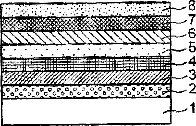
[0080]First, a transparent glass substrate (Corning 1713, 30mm×30mm, thickness 0.8mm) was prepared, and a thin film made of ITO was deposited on the glass substrate with a thickness of 340 Å by sputtering to form an anode. Then, a thin film composed of copper phthalocyanine (trade name P1005) manufactured by Tokyo Kasei Co., Ltd. (trade name P1005) was deposited on the anode to a thickness of 10 Å to form a hole injection layer. Next, a thin film of NPD (trade name 55, 669-6) manufactured by Aldrich was deposited to a thickness of 1000 Å on the hole injection layer by vapor deposition to form a hole transport layer. Then Alq3 (trade name T203) manufactured by Tongren Chemical was purified by sublimation. On the hole injection layer, a thin film composed of purified Alq3 was deposited to a thickness of 500 Å by evaporation to form a light emitting layer. Next, add 50mg Na@C prepared by Ideal Star 60 After ...
Embodiment 2
[0081] (Manufacture of light-emitting element related to Example 2)
[0082] First, a transparent glass substrate (Corning 1713, 30 mm x 30 mm, thickness 0.8 mm) was prepared, and a thin film made of ITO was deposited on the glass substrate to a thickness of 340 Å by sputtering to form an anode. Then, a thin film composed of copper phthalocyanine (trade name P1005) manufactured by Tokyo Chemical Industry Co., Ltd. (trade name P1005) was deposited on the anode to a thickness of 10 Å to form a hole injection layer. Next, a thin film made of NPD (trade name 55, 669-6) manufactured by Aldrich was deposited to a thickness of 1000 Å by vapor deposition on the hole injection layer to form a hole transport layer. Then Alq3 (trade name T203) manufactured by Tongren Chemical was purified by sublimation. On the hole injection layer, a thin film composed of purified Alq3 was deposited to a thickness of 500 Å by evaporation to form a light emitting layer. Then, 20 mg of PBD (trade name 2...
PUM
 Abstract
Description
Claims
Application Information


