Chip packing structure, chip structure and method for forming chip

A chip packaging and chip technology, applied in the fields of semiconductor/solid-state device manufacturing, electrical components, electrical solid-state devices, etc., can solve the problem of chip 120 pollution, etc., to prevent primer from creeping, control quality and cost, chip structure and chip Create simple effects

Active Publication Date: 2007-11-21
ADVANCED SEMICON ENG INC
View PDF0 Cites 5 Cited by
  • Summary
  • Abstract
  • Description
  • Claims
  • Application Information

AI Technical Summary

Problems solved by technology

A plurality of connection pads 112 are formed on a surface 111 of the carrier 110. The chip 120 is combined on the surface 111 of the carrier 110 in a flip-chip manner. The chip 120 has an active surface 121 and a back surface 122. The active surface 121 of 120 has several welding pads 123, and several bumps 140 connect these connection pads 112 on the carrier 110 and these welding pads 123 on the chip 120, and the primer 130 is formed on the carrier 110 Between the chip 120 to protect these bumps 140, however, in the baking step, the viscosity of the primer 130 will reduce and flow along the side of the chip 120 and extend to the back 122 of the chip 120 (here Phenomenon is also known as glue climbing), thus causing the chip 120 to be polluted

Method used


Image

  • Chip packing structure, chip structure and method for forming chip
  • Chip packing structure, chip structure and method for forming chip
  • Chip packing structure, chip structure and method for forming chip

Examples


Embodiment Construction

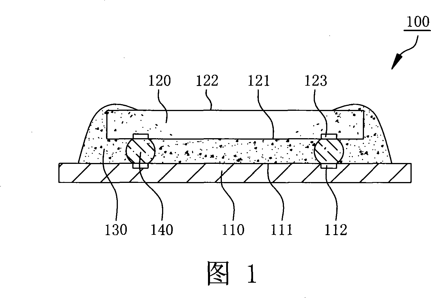
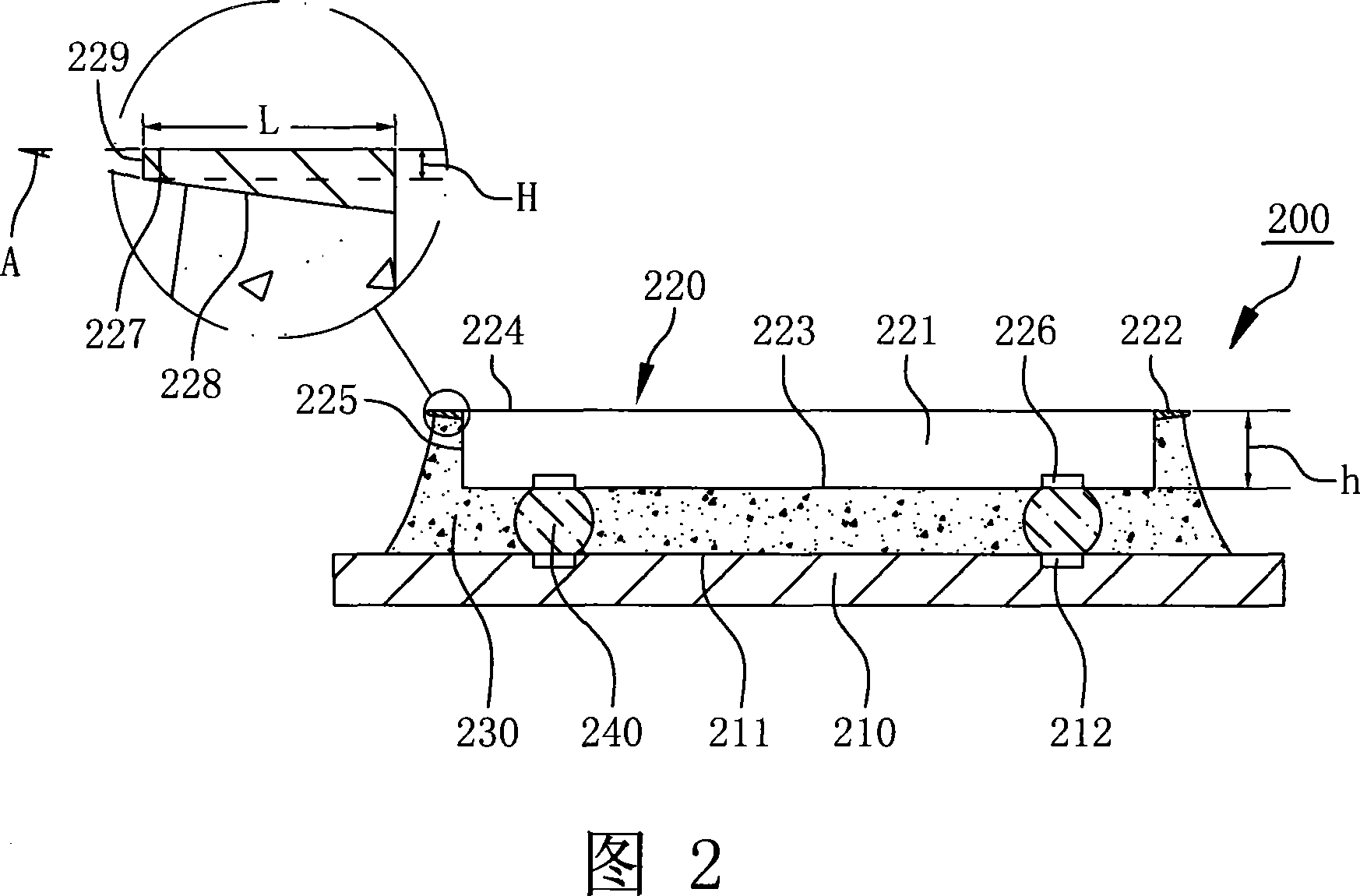
[0014] Please refer to FIG. 2 , a specific embodiment of the present invention discloses a chip packaging structure 200 , which includes a carrier 210 , a chip 220 and a primer 230 . The carrier 210 has a surface 211 on which a plurality of connection pads 212 are formed. The chip 220 is disposed on the surface 211 of the carrier 210 and electrically connected to the carrier 210. The chip 220 includes a chip Body 221 and a rubber blocking portion 222. The chip body 221 has an active surface 223, a back surface 224 and at least one side 225 between the active surface 223 and the back surface 224. Several solder joints are formed on the active surface 223. Pads 226, in addition, the chip 220 also includes several bumps 240, these bumps 240 are arranged on the pads 226 of the active surface 223, the active surface 223 of the chip body 221 faces the carrier 210 surface 211, and are bonded to the connection pads 212 of the carrier 210 through the bumps 240, the glue stop 222 can be...


PUM


Abstract

This is a chip packing structure avoiding gel overflow. It includes a supporter, chip and base gel. The chip is of a gel blocking section and installed on the supporter. The blocking section is to one side of the chip, with a top and bottom face in an acute angle. The base gel is in between the supporter and the chip and blocked by the bottom face of the gel blocking section.

Description

technical field [0001] The present invention relates to a chip packaging structure, a chip structure and a chip forming method, and in particular to a chip packaging structure, a chip structure and a chip forming method capable of preventing the primer from creeping. Background technique [0002] In order to reduce the electronic signal transmission distance between the chip and the carrier and reduce the size of the packaged chip package structure, the chip is combined with the carrier in a flip-chip manner. As shown in FIG. 1 , the existing chip package structure 100 includes a carrier device 110, a chip 120 and a primer 130. A plurality of connection pads 112 are formed on a surface 111 of the carrier 110. The chip 120 is combined on the surface 111 of the carrier 110 in a flip-chip manner. The chip 120 has an active surface 121 and a back surface 122. The active surface 121 of 120 has several welding pads 123, and several bumps 140 connect these connection pads 112 on t...

Claims


Application Information

Patent Timeline
Patent Type & Authority Applications(China)
IPC IPC(8): H01L23/31H01L27/00H01L21/78
CPCH01L2224/16225H01L2224/26175H01L2224/32225H01L2224/73204H01L2924/10155H01L2924/00
Inventor 林家旭
Owner ADVANCED SEMICON ENG INC
Why Eureka
Try Eureka