Packaged LED and manufacturing method thereof

A LED chip and potting technology, which is applied in the direction of electrical components, circuits, semiconductor devices, etc., can solve problems such as failure, and achieve the effects of improving service life, increasing safety distance, and reducing short circuit

Inactive Publication Date: 2016-07-06
LIGHTKING TECH GRP CO LTD
View PDF3 Cites 0 Cited by
  • Summary
  • Abstract
  • Description
  • Claims
  • Application Information

AI Technical Summary

Problems solved by technology

[0002] With the rapid development of LED technology, the application of LED display screens is becoming more and more extensive. The market demand for high pixel density LED display screens has increased dramatically, and high pixel density LED display screens have higher requirements for the size of the LED lights used. Smaller and smaller, but the traditional small-sized LED light bracket with general structure, the junction of the copper lead frame and the plastic reflector cup (PPA) is wrapped by plastic injection molding, this kind of LED is easy to cause failure after long-term use

Method used


Image

  • Packaged LED and manufacturing method thereof
  • Packaged LED and manufacturing method thereof
  • Packaged LED and manufacturing method thereof

Examples


Embodiment Construction

[0033] The preferred embodiments of the invention will be further described in detail below.

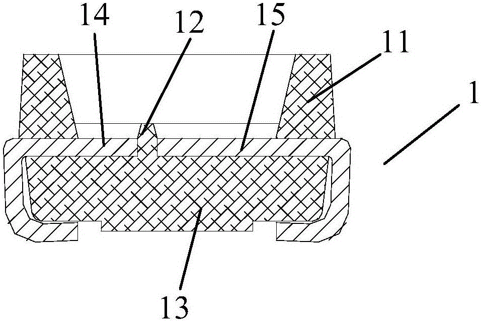
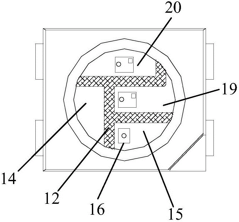
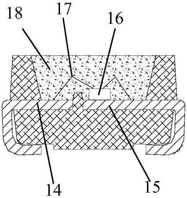
[0034] Such as Figures 1 to 4 As shown, a packaged LED of an embodiment includes a base 13, a reflective cup 11 (such as PPA plastic), an LED chip 16, an insulating boss 12 arranged on the base 13, and a plurality of conductive electrodes, Such as the positive conductive electrode 14, the conductive electrode 15, the conductive electrode 19 and the conductive electrode 20, the conductive electrode is set on the base 13, the reflective cup 11 is set on the conductive electrode, and the LED chip 16 is set In the reflective cup 11, the conductive electrode is used to electrically connect with the positive or negative electrode of the LED chip 16, the boss 12 is located in the reflective cup 11, and the boss 12 is arranged on the adjacent conductive electrode between, such as figure 2 As shown, bosses 12 are provided between the positive conductive electrode 14 and the conductive ele...


PUM


Abstract

The invention discloses a packaged LED and a manufacturing method thereof. The packaged LED comprises a base, a reflecting cup, an LED chip, a plurality of conductive electrodes and insulated bosses, wherein the conductive electrodes are arranged on the base; the reflecting cup is arranged on the conductive electrodes; the LED chip is arranged in the reflecting cup; the conductive electrodes are used for being electrically connected with a positive electrode or a negative electrode of the LED chip; the insulated bosses are arranged on the base and are located in the reflecting cup; and the bosses are arranged in gaps between adjacent conductive electrodes. According to the packaged LED, the silver migration distances among the conductive electrodes can be effectively increased through the bosses; short circuits among the conductive electrodes are reduced; and the service lifetime of the packaged LED is prolonged. Particularly, improvement of the manufacturing first-pass yield and reduction of the out-of-control ratio of an LED surface-mounted lamp which is smaller than 2.1mm*2.1mm in size are facilitated.

Description

【Technical field】 [0001] The invention relates to a packaged LED and a manufacturing method thereof. 【Background technique】 [0002] With the rapid development of LED technology, the application of LED display screens is becoming more and more extensive. The market demand for high pixel density LED display screens has increased dramatically, and high pixel density LED display screens have higher requirements for the size of the LED lights used. Smaller and smaller, but the traditional small-sized LED light bracket with general structure, the junction of the copper lead frame and the plastic reflector cup (PPA) is wrapped by plastic injection molding. This kind of LED is prone to failure after long-term use. 【Content of invention】 [0003] After research, it was found that in the above-mentioned existing LED lamps, there is a physical gap between the copper lead frame and the plastic reflector (PPA). Stress, the physical gap will become larger. Finally, during the applica...

Claims


Application Information

Patent Timeline
IPC IPC(8): H01L33/48H01L33/40H01L33/00
CPCH01L33/48H01L33/40H01L2933/0016H01L2933/0033
Inventor 邹启兵齐扬阳罗新房
Owner LIGHTKING TECH GRP CO LTD
Why Eureka
Try Eureka