Method for dressing polishing pads

A polishing pad and dresser technology, applied in the field of polishing pads, can solve the problems of unsatisfactory polishing pads and non-permanent polishing pad effects, and achieve the effects of increasing removal rate, improving plane parallelism, and improving surface quality

Inactive Publication Date: 2016-07-20
SILTRONIC AG
View PDF10 Cites 5 Cited by
  • Summary
  • Abstract
  • Description
  • Claims
  • Application Information

AI Technical Summary

Problems solved by technology

[0017] However, the effects achieved by known methods for conditioning polishing pads are generally not durable and do not produce satisfactory results for many of the polishing pads used

Method used


Image

  • Method for dressing polishing pads
  • Method for dressing polishing pads
  • Method for dressing polishing pads

Examples


Embodiment Construction

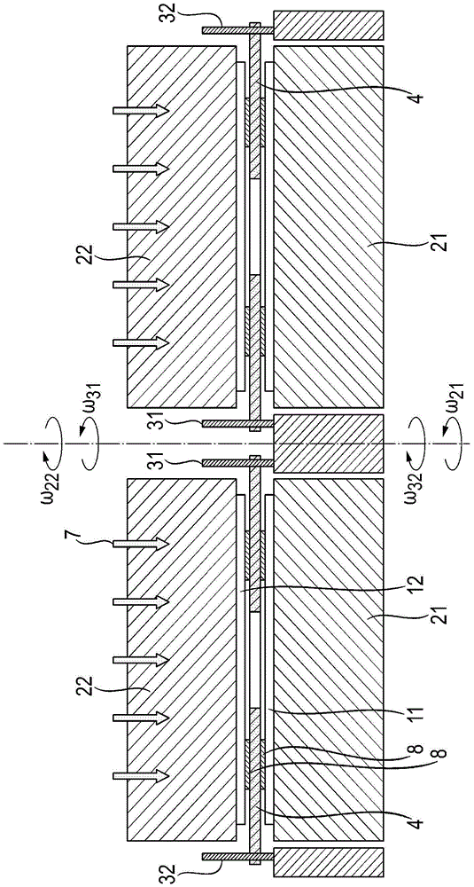
[0051] As already stated, the method according to the invention can be carried out both with a device for polishing a semiconductor wafer on one side and with a device for polishing a semiconductor wafer on both sides. If an apparatus for double-sided polishing of a semiconductor wafer is used, a dresser 4 can be used instead of the carrier plate used in the polishing process.

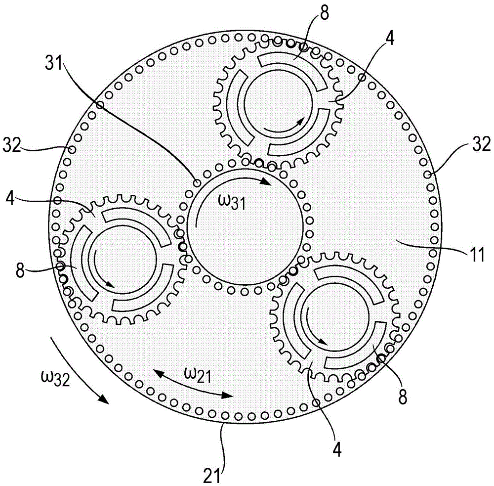
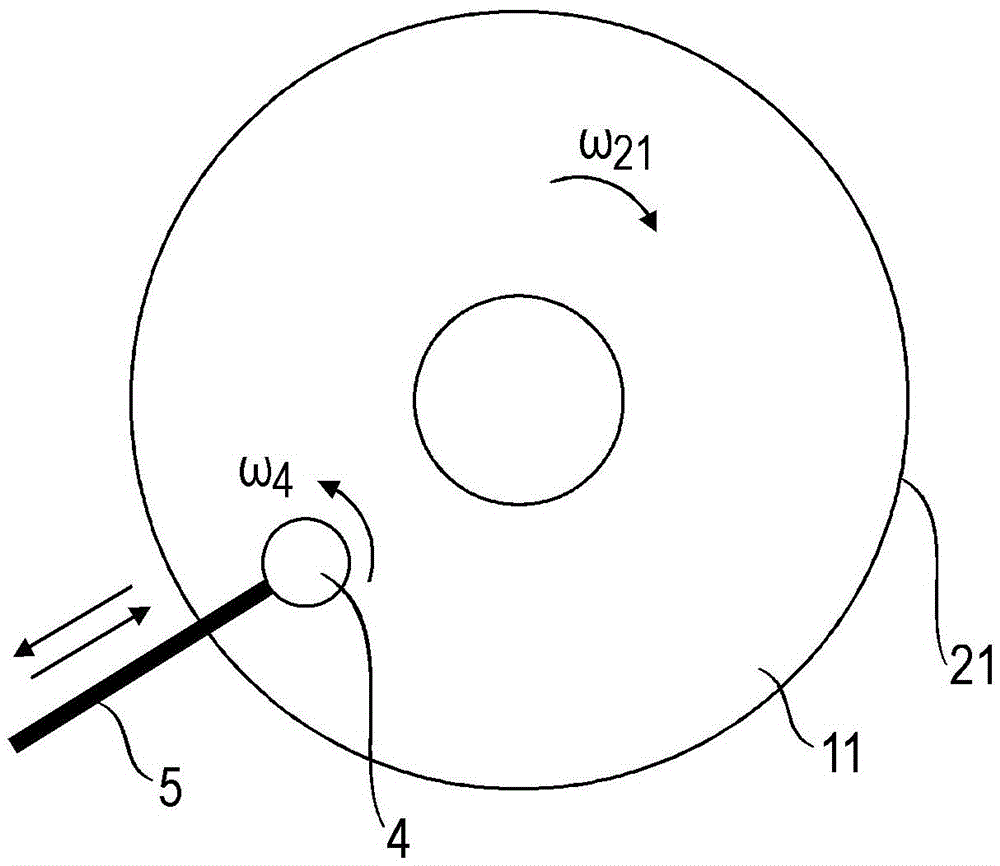
[0052] When using a device for double-sided polishing of semiconductor wafers, it is preferred to use an annular or disk-shaped dresser 4 with a peripheral gear ring in tooth mesh with an internal gear 31 and an external gear 32 . The rotational movement of the dresser 4 necessary for multidirectional dressing is ensured by the rotation of the two pinwheels. The side of the dresser 4 facing the upper polishing cloth 12 and the side of the dresser 4 facing the lower polishing cloth 11 are in each case preferably equipped with at least one dressing element 8 .

[0053] In a further embodiment of simult...


PUM


Abstract

A method dresses one polishing cloth or two polishing pads (11, 12) simultaneously, in which a polishing cloth has been applied to a polishing plate (21, 22), with at least one dresser (4), which is equipped with at least one dressing element (8), this at least one dressing element (8) being in contact with the at least one polishing cloth (11, 12) to be dressed, wherein the at least one polishing plate (21, 22) is rotated with a relative rotational speed and the at least one dresser (4) is rotated with a relative rotational speed and at least two different combinations of directions of rotation of the two pairs of polishing plates (21, 22) and pin wheels (31, 32) are executed during the simultaneous dressing of two polishing pads (11, 12) or during the dressing of one polishing cloth (11) of the polishing plate (21) and of the at least one dresser (4).

Description

technical field [0001] The invention relates to a method for conditioning a polishing pad (cloth), especially a polishing pad used in polishing semiconductor wafers. Background technique [0002] For electronic devices, microelectronics and microelectromechanical devices, semiconductor wafers are required as raw materials, and these semiconductor wafers must meet the requirements for overall and local flatness, flatness on one side (nano-layout), roughness and cleanliness. extreme requirements. Semiconductor wafers are such as single-element semiconductors (silicon, germanium), compound semiconductors (e.g., comprising an element from the third main group of the periodic table, such as aluminum, gallium, or indium, and a fifth main group from the periodic table. A thin slice of semiconductor material such as an element of the group such as nitrogen, phosphorus or arsenic) or its compound (such as Sil-xGex, 0<x<1). [0003] Semiconductor wafers are produced through a ...

Claims


Application Information

Patent Timeline
Patent Type & Authority Applications(China)
IPC IPC(8): B24B53/017B24B37/24
CPCB24B37/24B24B53/017B42D1/06B24B49/18B24B53/003B24B53/02B24B53/12
Inventor V·杜奇克T·奥尔布里希L·米斯图尔M·施纳普奥夫
Owner SILTRONIC AG
Why Eureka
Try Eureka