Package method and package structure for fingerprint identification chip

A fingerprint identification and packaging method technology, which is applied in the manufacture of electrical components, electrical solid devices, semiconductor/solid devices, etc., can solve the problems of large space occupation and high cost of wire bonding process, and achieve the solution of large space occupation and reduced relative height , cost reduction effect

Inactive Publication Date: 2016-07-20
SHENZHEN CHIPSBANK TECH
View PDF6 Cites 4 Cited by
  • Summary
  • Abstract
  • Description
  • Claims
  • Application Information

AI Technical Summary

Problems solved by technology

[0005] The invention provides a packaging method and packaging structure of a fingerprint identification chip, which are used to solve the problems of high cost and large space occupation of the existing wire bonding process

Method used


Image

  • Package method and package structure for fingerprint identification chip
  • Package method and package structure for fingerprint identification chip
  • Package method and package structure for fingerprint identification chip

Examples


Embodiment Construction

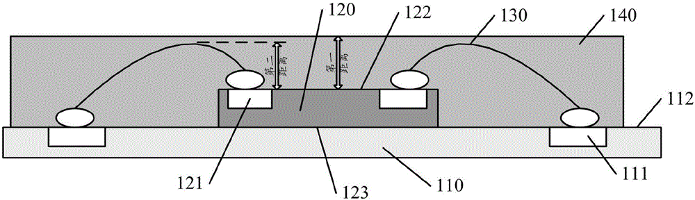
[0034] In the prior art, the packaging structure of the fingerprint identification chip, please continue to refer tofigure 1 , including: a substrate 110, the substrate 110 has a first surface 112, the first surface 112 of the substrate 110 has a plurality of substrate pads 111; a fingerprint identification chip 120, the fingerprint identification chip has a second surface 122, and the second surface 122 opposite The third surface 123, the third surface 123 is located on the first surface 112 of the substrate, the second surface 122 has several chip pads 121; conductive lines 130, the two ends of the conductive lines 130 are electrically connected to the substrate pads 111 and the chip pads 121 respectively Connect, wherein the vertical distance from the highest point of the conductive line to the second surface 122 is the second distance; the plastic sealing layer 140, the plastic sealing layer 140 is located on the surface of the substrate 110 and the fingerprint recognition c...


PUM


Abstract

The embodiment of the invention discloses a package method and a package structure for a fingerprint identification chip. The package method comprises the following steps: providing a substrate; trepanning the substrate to obtain a target hole; fixing the fingerprint identification chip in the target hole, making the third face of the fingerprint identification chip face to the same direction as the first face of the substrate, wherein the third face and the first face are located on the same plane, and the third face is provided with an induction area and a chip bonding pad; welding a substrate bonding pad with the chip bonding pad to form an electric connection, wherein the substrate bonding pad is located on the first face of the substrate; and plastic packaging the fingerprint identification chip. The embodiment of the invention further provides a package structure for the fingerprint identification chip. According to the package method disclosed by the invention, the fingerprint identification chip is embedded in the target hole of the substrate, and the chip bonding pad and the substrate bonding pad are located on the same plane, so the electric interconnection of the chip bonding pad and the substrate bonding pad can be realized by the welding process to reduce the cost, and solve the problem of large occupancy space of the trepanning process.

Description

technical field [0001] The invention relates to the technical field of semiconductor manufacturing, in particular to a packaging method and packaging structure of a fingerprint recognition chip. Background technique [0002] With the development of science and technology, the information security of various electronic products, especially mobile terminals, has become the focus of technological development. Due to the characteristics of invariance, uniqueness and convenience of human fingerprints, fingerprint recognition technology has the characteristics of safety, reliability, simple and convenient use, etc., making fingerprint recognition technology widely used in various fields of protecting personal information. [0003] The existing fingerprint identification device extracts the user's fingerprint through the fingerprint identification chip, and converts the user's fingerprint into an electrical signal output to obtain the user's fingerprint information. figure 1 It is...

Claims


Application Information

Patent Timeline
Patent Type & Authority Applications(China)
IPC IPC(8): H01L21/56H01L23/00
CPCH01L21/56H01L24/10H01L24/81H01L2224/04105H01L2224/24137H01L2224/24227H01L2224/48091H01L2924/00014
Inventor 张华龙李华伟
Owner SHENZHEN CHIPSBANK TECH
Why Eureka
Try Eureka