Non-volatile Memory And Fabricating Method Thereof

A non-volatile, manufacturing method technology, used in semiconductor/solid-state device manufacturing, electric solid-state devices, semiconductor devices, etc., can solve the problems of complex manufacturing process of non-volatile memory structure and difficult to control the size of components

Active Publication Date: 2016-07-20
POWERCHIP SEMICON MFG CORP
View PDF3 Cites 4 Cited by
  • Summary
  • Abstract
  • Description
  • Claims
  • Application Information

AI Technical Summary

Problems solved by technology

[0006] However, the manufacturing process of the non-volatile memory structure with split gates is too complicated and it is difficult to control the size of the components (such as the line width of the selection gate), which is an urgent problem to be solved in the industry.

Method used


Image

  • Non-volatile Memory And Fabricating Method Thereof
  • Non-volatile Memory And Fabricating Method Thereof
  • Non-volatile Memory And Fabricating Method Thereof

Examples


Embodiment Construction

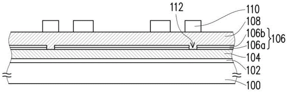
[0048] Figure 1A to Figure 1E It is a sectional view of the manufacturing process of the non-volatile memory according to an embodiment of the present invention.

[0049] First, please refer to Figure 1A , the dielectric layer 102 can be optionally formed on the substrate 100 . The substrate 100 is, for example, a silicon substrate. The material of the dielectric layer 102 is, for example, silicon oxide. The dielectric layer 102 is formed by, for example, thermal oxidation or chemical vapor deposition.

[0050]Next, a conductive material layer 104 , a dielectric material layer 106 , a conductive material layer 108 and a patterned mask layer 110 are sequentially formed on the dielectric layer 102 .

[0051] The material of the conductive material layer 104 is, for example, a conductive material such as doped polysilicon. The method for forming the conductive material layer 104 is, for example, chemical vapor deposition.

[0052] The dielectric material layer 106 is, for ...


PUM


Abstract

A non-volatile memory including a substrate, a first stacked structure, a second stacked structure, a fifth conductive layer, a first doped region, and a second doped region is provided. The first stacked structure includes a first conductive layer and a second conductive layer stacked on the substrate in order and isolated from each other. The second stacked structure is separately disposed from the first stacked structure and includes a third conductive layer and a fourth conductive layer stacked on the substrate in order and connected to each other. The fifth conductive layer is disposed on the substrate at one side of the first stacked structure away from the second stacked structure. The first doped region is disposed in the substrate below the fifth conductive layer. The second doped region is disposed in the substrate at one side of the second stacked structure away from the first stacked structure.

Description

technical field [0001] The present invention relates to a memory and its manufacturing method, and in particular to a non-volatile memory and its manufacturing method. Background technique [0002] Non-volatile memory elements are widely used in personal computers and electronic devices due to their advantages that the stored data will not disappear even after the power is turned off. [0003] A typical non-volatile memory device includes a floating gate and a control gate. The control gate is arranged on the floating gate, and a dielectric layer is respectively arranged between the floating gate and the substrate, and between the floating gate and the control gate. [0004] When erasing the non-volatile memory, there is a problem of over-erase, which leads to misjudgment of data. Therefore, in order to solve the problem of over-erasing of devices, many non-volatile memories adopt a split gate design. [0005] The non-volatile memory structure with split gate is character...

Claims


Application Information

Patent Timeline
Patent Type & Authority Applications(China)
IPC IPC(8): H01L27/115H01L21/8247H01L21/28
CPCH01L29/42328H01L29/267H01L29/40114H10B41/30
Inventor 许正源张振福陈辉煌应宗桦
Owner POWERCHIP SEMICON MFG CORP
Why Eureka
Try Eureka