Thin film deposition assembly and thin film deposition device

A technology of thin film deposition and components, applied in ion implantation plating, metal material coating process, coating, etc., can solve the problems that it is difficult to deal with large-scale substrate mass production and small effective deposition area, so as to improve uniformity, The effect of large effective deposition area

Inactive Publication Date: 2016-07-27
WUHAN CHINA STAR OPTOELECTRONICS TECH CO LTD
View PDF6 Cites 6 Cited by
  • Summary
  • Abstract
  • Description
  • Claims
  • Application Information

AI Technical Summary

Problems solved by technology

[0005] However, when the existing pulsed laser deposition technology is used to fabricate thin films in flexible OLED display devices, the effective deposition area of ​​the existing pulsed laser deposition device is small, it is difficult to meet the needs of mass production of large-size substrates, and for large-size substrates thin film deposition, the uniformity of the deposited film is also challenged
In addition, the existing pulsed laser deposition equipment is difficult to co-deposit thin films with multiple targets

Method used


Image

  • Thin film deposition assembly and thin film deposition device
  • Thin film deposition assembly and thin film deposition device
  • Thin film deposition assembly and thin film deposition device

Examples


Embodiment Construction

[0022] Hereinafter, embodiments of the present invention will be described in detail with reference to the accompanying drawings. This invention may, however, be embodied in many different forms and should not be construed as limited to the specific embodiments set forth herein. Rather, the embodiments are provided to explain the principles of the invention and its practical application, thereby enabling others skilled in the art to understand the invention for various embodiments and with various modifications as are suited to particular intended uses.

[0023] In the drawings, the thicknesses of layers and regions are exaggerated for clarity of components. Like reference numerals refer to like elements throughout the drawings.

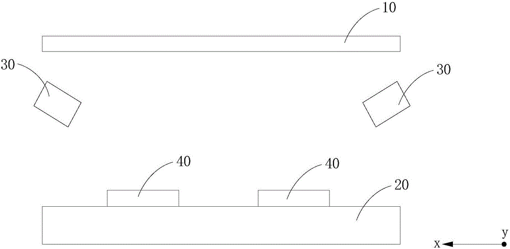
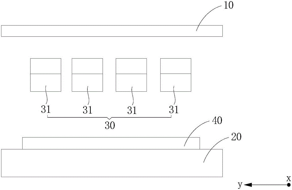
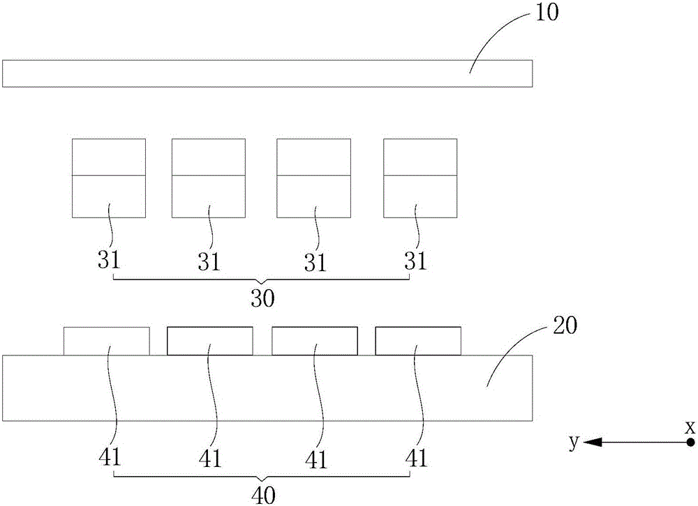
[0024] figure 1 is a structural front view of a thin film deposition assembly according to an embodiment of the present invention. figure 2 yes figure 1 left view of .

[0025] refer to figure 1 and figure 2 , The thin film deposition assemb...


PUM


Abstract

The invention discloses a thin film deposition assembly. The thin film deposition assembly comprises a deposition substrate (10), a target material bearing disk (20), a plurality of target materials (40) arranged on the surfaces, facing the deposition substrate (10), of the target material bearing disk (2) and arranged at intervals in the first direction, and a plurality of laser radiation source sets (3) arranged between the deposition substrate (10) and the target material bearing disk (20), wherein the deposition substrate (10) and the target material bearing disk (20) are oppositely arranged; the laser radiation source sets (30) correspond to the target materials (40) one to one; each laser radiation source set (30) comprises a plurality of laser radiations sources (31) arranged at intervals in the second direction; and the first direction intersects with the second direction. The invention further discloses a thin film deposition device. According to the thin film deposition assembly and the thin film deposition device, effective deposition areas are large, and therefore the large-batch production requirement of large-size substrates can be met, and by means of the design of point arrangement of the laser radiation sources and the movement manner of the target material bearing disk and/or the deposition substrate in the thin film deposition process, the thin film deposition evenness is improved.

Description

technical field [0001] The invention belongs to the technical field of thin film manufacturing equipment, and in particular relates to a thin film deposition component and a thin film deposition device. Background technique [0002] Compared with the current mainstream liquid crystal display technology, organic light-emitting (OLED) display technology has outstanding advantages such as high contrast, wide color gamut, flexibility, thinness, and energy saving. In recent years, OLED display technology has gradually become popular in mobile devices such as smartphones and tablet computers, flexible wearable devices such as smart watches, large-size curved TVs, and white lighting, and its development momentum is strong. [0003] At present, flexible OLED display devices have been put into commercial operation. Flexible OLED devices need to use flexible thin film encapsulation technology (TFE, Thin Film Encapsulation), whether water and oxygen can be effectively blocked is a key...

Claims


Application Information

Patent Timeline
Patent Type & Authority Applications(China)
IPC IPC(8): C23C14/28
CPCC23C14/28
Inventor 沐俊应
Owner WUHAN CHINA STAR OPTOELECTRONICS TECH CO LTD
Why Eureka
Try Eureka