A routing structure about dram clock tree
A line structure and clock technology, applied in the field of DRAM clock tree line structure, to achieve the effect of maintaining consistency and reducing impact
- Summary
- Abstract
- Description
- Claims
- Application Information
AI Technical Summary
Problems solved by technology
Method used
Image
Examples
Embodiment Construction
[0022] The clock clock signal mentioned in the present invention can be extended to many important and high-frequency signals. For example, the output signal of the oscillator, the output signal of the voltage-controlled oscillator of the phase-locked loop, the clock signal of the high-definition multimedia interface, etc. can all be used in the routing optimization method mentioned in the present invention.
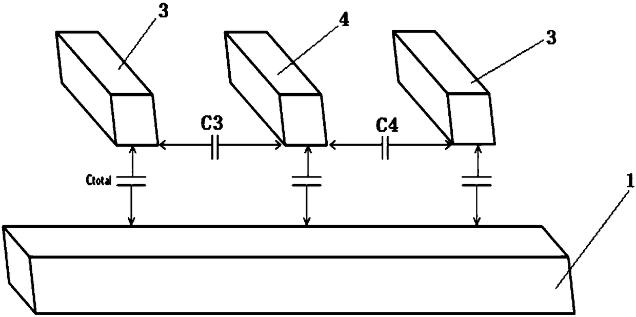
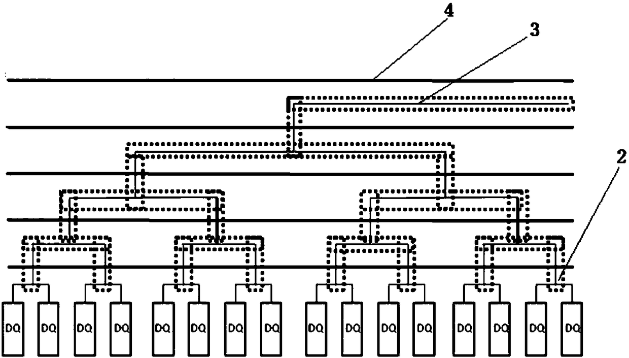
[0023] Such as image 3 Shown is a schematic diagram of the wiring structure of the DRAM clock tree of the present invention; Figure 4 It is a cross-section of the DRAM clock tree routing structure of the present invention, showing the partial tree structure of the clock tree after optimization, the isolation lines and the relationship with the substrate. It specifically includes a substrate, a clock tree layer, and an isolation unit arranged between the substrate and the clock tree layer. The isolation unit includes a parasitic capacitance C1, a parasitic capacitance ...
PUM
 Abstract
Description
Claims
Application Information


