Clock Delay Control Method Based on Printed Circuit Board
A printed circuit board, clock delay technology, applied in the direction of multi-terminal pair network, impedance matching network, etc., can solve the problems of waveform overshoot and ringing, complex peripheral circuits, waveform distortion, etc., to save device costs and broad application prospects , the effect of shielding crosstalk
- Summary
- Abstract
- Description
- Claims
- Application Information
AI Technical Summary
Problems solved by technology
Method used
Image
Examples
Embodiment Construction
[0024] A flexible, economical and efficient board-level clock delay control method is realized. A pure hardware clock delay control method based on a printed circuit board is provided. Using this method can realize the equivalent sampling of the clock, and then improve the precision of the data acquisition system.
[0025] The method for controlling the clock delay based on the printed circuit board will be further described in detail below through two embodiments.
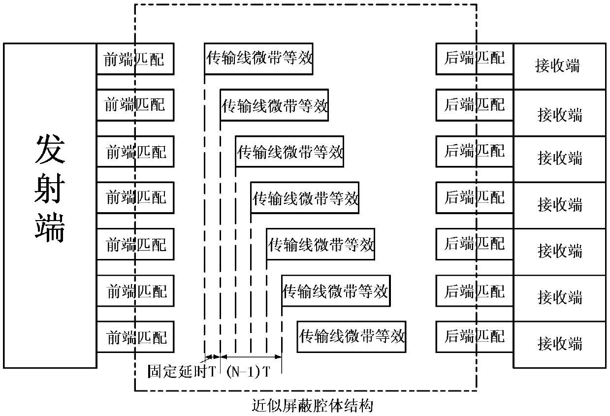
[0026] Such as figure 1 , 2 Shown, embodiment 1, this method adopts following technical scheme:
[0027] 1. Build a ring shunt circuit. The transmitting end is used as the port of the clock output end, and the receiving end is used as the port of the clock input load end. The transmitter joins the corresponding power supply network and ground network as the reference voltage according to the specific type of clock used.
[0028] 2. An approximate shielding structure is built in the printed circuit board to s...
PUM
 Abstract
Description
Claims
Application Information

