
A non-volatile memory processing circuit and method

A technology of non-volatile memory and processing circuit, which is applied in the field of memory processing and can solve the problems of low reading accuracy of storage unit data and reading errors of storage unit data.

Active Publication Date: 2021-07-09
GIGADEVICE SEMICON XIAN INC +1
View PDF6 Cites 0 Cited by
  • Summary
  • Abstract
  • Description
  • Claims
  • Application Information

AI Technical Summary

Problems solved by technology

[0004] However, the inventor found in the process of studying the above-mentioned technical solution that the above-mentioned technical solution has the following defects: each BL voltage will be affected by the connected crosstalk capacitance, which will cause some memory cell data reading errors, and the data reading of the storage cells The accuracy is not high

Method used


Image

  • A non-volatile memory processing circuit and method
  • A non-volatile memory processing circuit and method
  • A non-volatile memory processing circuit and method

Examples


Embodiment 1

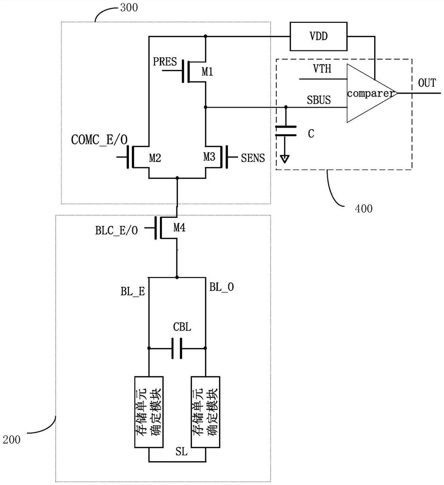
[0055] refer to figure 1 , shows a non-volatile memory processing circuit, which may specifically include: a charging circuit 300 , a comparison circuit 400 , and a storage unit selection circuit 200 .

[0056]Wherein, the memory cell selection circuit includes at least one pair of memory cell strings; each pair of memory cell strings includes a first memory cell string and a second memory cell string, and the bit line BLO of the first memory cell string and the A capacitor CBL is connected between the bit lines BLE of the second memory cell string; each of the memory cell strings is connected to a source line SL.

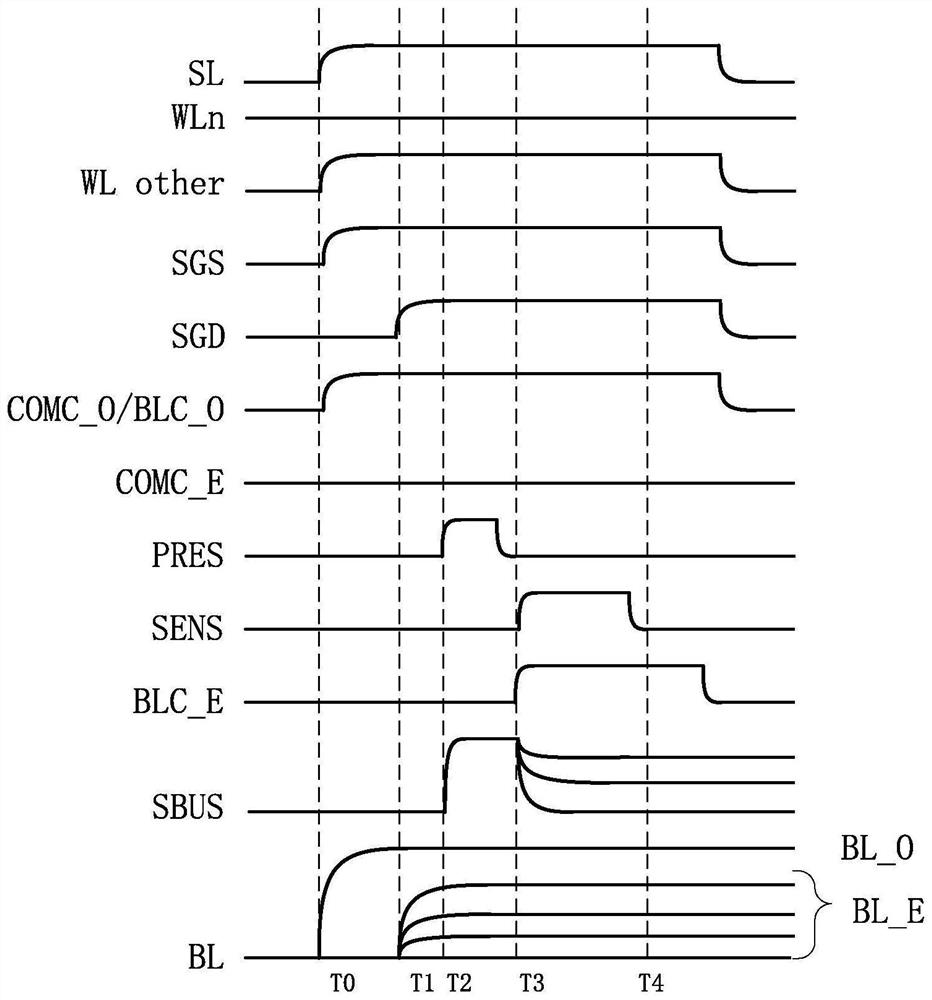
[0057] The charging circuit is connected to the storage unit selection circuit, and is used to initially charge the bit line BLO of the first storage unit string in the storage unit selection circuit; and charge the source line SL; After the bit line BLO of the first memory cell string is charged stably, charge the bit line BLE of the second memory cell string thr...

Embodiment 2

[0079] refer to Figure 4 , which shows a non-volatile memory processing method, which is applied to any of the above-mentioned non-volatile memory processing circuits, and may specifically include:

[0080] Step 401: Determine the storage unit to be detected in the storage unit selection circuit; wherein, the storage unit string where the storage unit to be detected is located is a second storage unit string.

[0081] In the embodiment of the present invention, the storage unit selection circuit can select the storage unit to be detected. In order to clearly illustrate the embodiment of the present invention when reading data from the storage unit, the paired storage unit strings are distinguished, so the storage unit to be detected is located The string of storage cells is called the second string of storage cells, and the string paired with the second string of storage cells is the first string of storage cells.

[0082]As a preferred implementation of the embodiment of th...


PUM


Abstract

An embodiment of the present invention provides a non-volatile memory processing circuit and method, the method comprising: a charging circuit connected to a storage unit selection circuit for charging the bit line of the first storage unit string; and charging the source line ; After the bit line of the first memory cell string is charged stably, the bit line of the second memory cell string is charged through the source line; the charging circuit is connected with the comparison circuit, and is used for when the bit line of the second memory cell string is charged stably , charge the comparison circuit, and, when the comparison circuit is charged stably, end the charging of the comparison circuit and the storage unit selection circuit; the storage unit selection circuit and the comparison circuit form a current loop, so that the comparison circuit outputs a high level according to the current loop or low level. The embodiment of the present invention shields the capacitance crosstalk between the first storage unit string and the second storage unit string, so when the storage unit in the non-volatile memory is read, the data of each storage unit can be accurately read .

Description

technical field [0001] The invention relates to the technical field of memory processing, in particular to a nonvolatile memory processing circuit and method. Background technique [0002] With the development of various electronic devices and embedded systems, non-volatile memory devices are widely used in electronic products. Taking the non-volatile memory NAND flash memory (NAND Flash Memory) as an example, the NAND memory is composed of a plurality of storage cells (cells), and the storage cells can be negative threshold storage cells, that is, the storage cells whose conduction threshold voltage is a negative value; It can be a positive threshold memory cell, that is, a memory cell whose on-threshold voltage is positive; according to the on-current of the memory cell during operation, the data state of the memory cell can be read, such as erased state, programmed state, etc. [0003] In the prior art, when reading data from each storage unit of a non-volatile memory, a...

Claims


Application Information

Patent Timeline
Patent Type & Authority Patents(China)
IPC IPC(8): G11C16/24G11C16/26G11C16/34
CPCG11C16/24G11C16/26G11C16/3404
Inventor 马思博贾少旭舒清明
Owner GIGADEVICE SEMICON XIAN INC
Learn More