Organic electroluminescent device

An electroluminescent device and luminescence technology, which is applied in the direction of electric solid-state devices, electrical components, semiconductor devices, etc., can solve the problems of poor display effect and achieve the effect of wide selection of materials and high light extraction efficiency

Active Publication Date: 2016-07-27
GUAN YEOLIGHT TECH CO LTD
View PDF14 Cites 4 Cited by
  • Summary
  • Abstract
  • Description
  • Claims
  • Application Information

AI Technical Summary

Problems solved by technology

[0008] For this reason, what the present invention intends to solve is the problem that the existing mirror screen body has poor display effect due to the existence of surface plasmon mode, ITO / Glass and Glass / air three kinds of light losses, and provides an organic electroluminescent device, which focuses on the surface The plasma mode solves the light loss of other scattering interfaces at the same time, that is, reduces the light loss of the three modes at the same time, and maximizes the light output efficiency

Method used


Image

  • Organic electroluminescent device
  • Organic electroluminescent device
  • Organic electroluminescent device

Examples


Embodiment 1

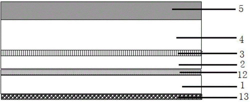
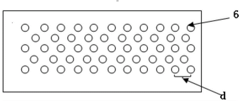
[0061] Embodiment 1 The second light extraction layer is arranged between the ITO and the organic functional layer NPB, the cross-section of the micro-pillars 6 is circular, and the cross-sectional area of ​​all the micro-pillars 6 is 3% of the total area of ​​the second light extraction layer , the distance d between adjacent micropillars is 100 μm, and the device structure is as follows:

[0062] Glass / ITO / cylindrical light extraction layer(50nm) / NPB(80nm) / Alq 3 :2%C545T(30nm) / Alq 3 (30nm) / LiF(1nm) / Al(150nm)

Embodiment 2

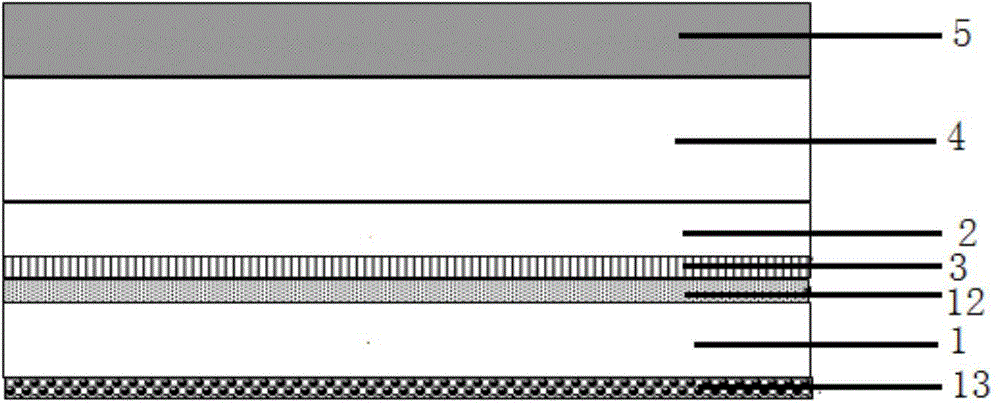
[0063]Embodiment 2: The structure of the device is the same as that of Comparative Example 1, except that the first light extraction layer (scattering layer) is prepared by adding at the interface between ITO and glass. The main body of the first light extraction layer (scattering layer) is a positive photoresist with a refractive index of 1.5, doped with high-refractive scattering particles of titanium dioxide, and the particle size is about 400nm. The high-refractive index particles account for 20wt% of the polymer body layer. The device structure as follows.

[0064] Glass / first light extraction layer (scattering layer) / ITO / NPB(80nm) / Alq 3 :2%C545T(30nm) / Alq 3 (30nm) / LiF(1nm) / Al(150nm)

Embodiment 3

[0065] Example 3: The main structure is the same as Comparative Example 1, except that after the device is prepared, a microlens film is pasted on the light-emitting surface of the device. The microlens is a densely packed hemispherical structure with a lens diameter of 50 μm. It can be prepared by nanoimprinting. The device structure as follows.

[0066] Microlens film / Glass / ITO / NPB(80nm) / Alq 3 :2%C545T(30nm) / Alq 3 (30nm) / LiF(1nm) / Al(150nm)


PUM


Abstract

The invention discloses an organic electroluminescent device, comprising a substrate and an organic electroluminescent unit arranged on the substrate, wherein the organic electroluminescent unit comprises a first electrode layer, an organic functional layer and a second electrode layer stacked in sequence, and the first electrode layer is arranged close to the substrate; the organic electroluminescent device further comprises a second light extraction layer arranged between the substrate and the second electrode layer, a plurality of different interface regions for changing the flatness of a second electrode reflecting interface are formed in the second light extraction layer, and the different interface regions occupy 0.1-30% of the area of the second light extraction layer. The device has high definition while keeping mirror reflection.

Description

technical field [0001] The invention relates to the field of organic electroluminescence, in particular to an organic electroluminescence device with high light extraction efficiency. Background technique [0002] After nearly 30 years of development, organic electroluminescent devices (English full name OrganicLightEmittingDevice, referred to as OLED) as the next generation of lighting and display technology, has a wide color gamut, fast response, wide viewing angle, no pollution, high contrast, planarization And other advantages, has been applied to a certain extent in lighting and display. A typical organic electroluminescent device generally includes a transparent substrate 1 , a first transparent electrode 3 , a second electrode 5 , and an organic functional layer 4 disposed between the two electrodes. Usually the cathode of the bottom-emitting OLED is a flat metal, which has a good reflection effect. The reflective surface can be applied in many fields, such as vanit...

Claims


Application Information

Patent Timeline
Patent Type & Authority Applications(China)
IPC IPC(8): H01L51/52H01L51/54H01L51/50
Inventor 张国辉董艳波王静李曼胡永岚
Owner GUAN YEOLIGHT TECH CO LTD
Why Eureka
Try Eureka