An organic electroluminescent device
An electroluminescence device and electroluminescence technology, which are applied in the direction of electro-solid devices, electrical components, semiconductor devices, etc., can solve the problems of poor display effect, etc., and achieve the effect of wide selection of materials and high light extraction efficiency.
- Summary
- Abstract
- Description
- Claims
- Application Information
AI Technical Summary
Problems solved by technology
Method used
Image
Examples
Embodiment 1
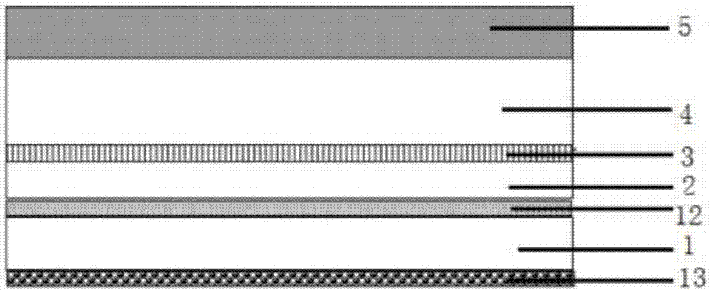
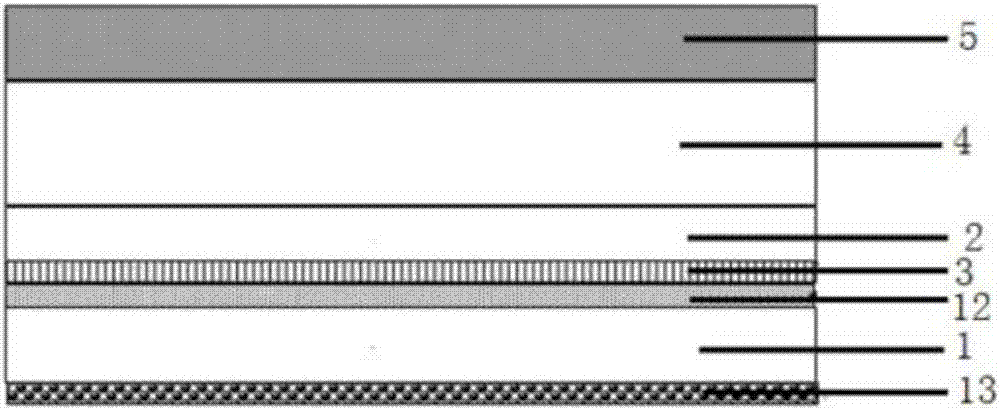
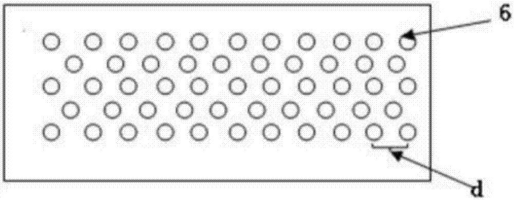
[0062] Embodiment 1 The second light extraction layer is arranged between the ITO and the organic functional layer NPB, the cross-section of the micro-pillars 6 is circular, and the cross-sectional area of all the micro-pillars 6 is 3% of the total area of the second light extraction layer , the distance d between adjacent micropillars is 100 μm, and the device structure is as follows:
[0063] Glass / ITO / cylindrical light extraction layer(50nm) / NPB(80nm) / Alq 3 : 2% C545T(30nm) / Alq3(30nm) / LiF(1nm) / Al(150nm)
Embodiment 2
[0064] Embodiment 2: The structure of the device is the same as that of Comparative Example 1, except that the first light extraction layer (scattering layer) is prepared by adding at the interface between ITO and glass. The main body of the first light extraction layer (scattering layer) is a positive photoresist with a refractive index of 1.5, doped with high-refractive scattering particles of titanium dioxide, and the particle size is about 400nm. The high-refractive index particles account for 20wt% of the polymer body layer. The device structure as follows.
[0065] Glass / first light extraction layer (scattering layer) / ITO / NPB(80nm) / Alq 3 : 2% C545T (30nm) / Alq 3 (30nm) / LiF(1nm) / Al(150nm)
Embodiment 3
[0066] Example 3: The main structure is the same as Comparative Example 1, except that after the device is prepared, a microlens film is pasted on the light-emitting surface of the device. The microlens is a densely packed hemispherical structure with a lens diameter of 50 μm. It can be prepared by nanoimprinting. The device structure as follows.
[0067] Microlens film / Glass / ITO / NPB(80nm) / Alq 3 : 2% C545T (30nm) / Alq 3 (30nm) / LiF(1nm) / Al(150nm)
PUM
 Abstract
Description
Claims
Application Information


