
Shutdown residual shadow elimination circuit and driving method thereof and display device

A technology for eliminating circuit and power-off afterimages, applied in static indicators, instruments, etc., can solve problems such as lowering the output voltage of the gate drive circuit, affecting the effect of power-off afterimage elimination, and unable to export the charge of the pixel electrodes in time

Active Publication Date: 2016-08-10
BOE TECH GRP CO LTD +1
View PDF7 Cites 18 Cited by
  • Summary
  • Abstract
  • Description
  • Claims
  • Application Information

AI Technical Summary

Problems solved by technology

However, when the display is turned off, the control signal input to the gate drive circuit is at a low level, so it is likely to pull down the output voltage of the gate drive circuit, which will cause the TFTs of some pixels to turn on and then turn off again, which will cause the pixel electrode The charge in the battery cannot be exported in time, which affects the effect of eliminating afterimage after shutdown

Method used


Image

  • Shutdown residual shadow elimination circuit and driving method thereof and display device
  • Shutdown residual shadow elimination circuit and driving method thereof and display device
  • Shutdown residual shadow elimination circuit and driving method thereof and display device

Examples


Embodiment 1

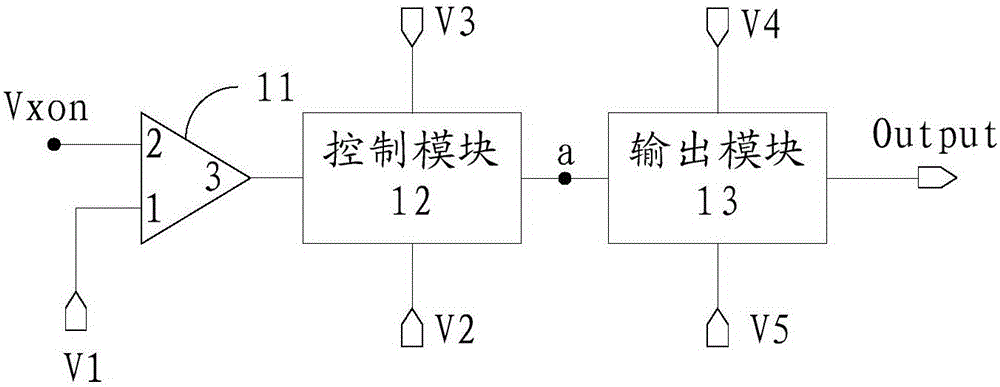
[0060] Embodiments of the present invention provide a shutdown afterimage elimination circuit, refer to figure 1 As shown, the power-off afterimage elimination circuit includes: a comparator 11 , a control module 12 and an output module 13 .

[0061] The inverting terminal 1 of the comparator 11 is connected to the first level terminal V1, and the non-inverting terminal 2 of the comparator is connected to the control voltage input terminal Vxon; When the output terminal 3 of the comparator 11 outputs a high-level voltage, when the input voltage of the non-inverting terminal 2 is less than or equal to the input voltage of the inverting terminal 1, the output terminal 3 of the comparator 11 outputs a low-level voltage.

[0062] The control module 12 is connected to the second level terminal V2, the third level terminal V4, the control node a and the output terminal 3 of the comparator 11, and is used to control the voltage of the node a when the output terminal 3 of the comparat...

Embodiment 2

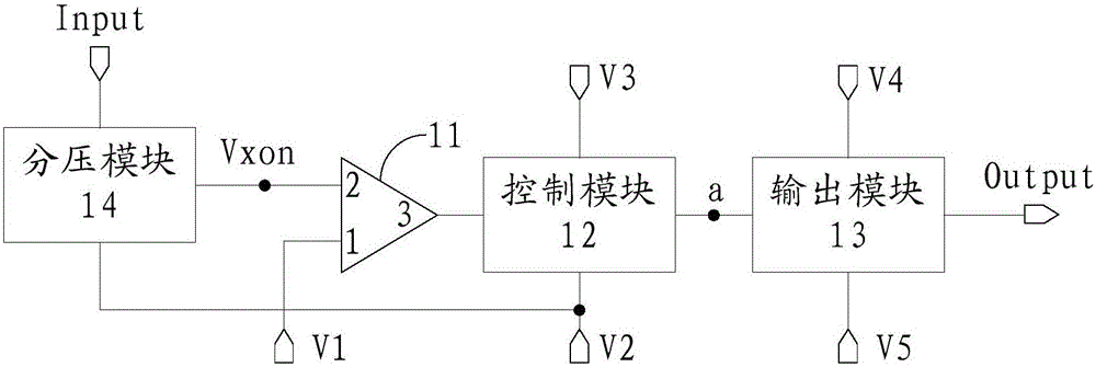
[0074] An embodiment of the present invention provides a specific circuit diagram of the above-mentioned power-off afterimage elimination circuit.

[0075] Specifically, refer to Figure 4 As shown, the control module 12 in the above embodiment includes: a first transistor T1;

[0076] The first terminal of the first transistor T1 is connected to the control node a and the second level terminal V2 , the second terminal of the first transistor T1 is connected to the third level terminal V3 , and the gate of the first transistor T1 is connected to the output terminal 3 of the comparator 11 .

[0077] The output module 13 includes: a second transistor T2 and a third transistor T3;

[0078] The first terminal of the second transistor T2 is connected to the fourth level terminal V4, the second terminal of the second transistor T2 is connected to the signal output terminal Output, and the gate of the second transistor T2 is connected to the control node a;

[0079] The first termi...

Embodiment 3

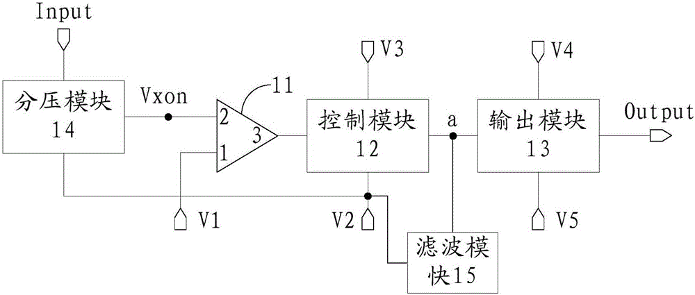
[0095] An embodiment of the present invention provides another specific circuit diagram of the above-mentioned power-off residual image elimination circuit.

[0096] Specifically, refer to Figure 5 As shown, wherein, the control module 12, the voltage divider module 14 and the filter module 15 are the same as those in the second embodiment, and to avoid redundant description, they will not be described in detail in this embodiment. The difference is that the output module 13 includes: an inverting unit 131, a fourth transistor T4 and a fifth transistor T5;

[0097] The input terminal of the inverting unit 131 is connected to the control node a, the output terminal of the inverting unit 131 is connected to the gate of the fifth transistor T5, and the inverting unit 131 is used to output the output terminal of the inverting unit 131 and the input of the inverting unit 131 The phase-opposite voltage of the voltage input at the terminal;

[0098] The first terminal of the fourt...


PUM


Abstract

The embodiment of the invention provides a shutdown residual shadow elimination circuit and a driving method thereof and a display device, relates to the technical field of display, and is used for preventing shutdown of TFT of pixels after power-on of the TFT of the pixels and then enhancing the effect of shutdown residual shadow elimination. The circuit comprises a comparator, a control module and an output module. The comparator is used for outputting high level voltage when same-end voltage is greater than reverse-end voltage and outputting low level voltage when the same-end input voltage is less than or equal to the reverse-end input voltage. The control module is used for leveling voltage of a control node and voltage of a second level end when the comparator outputs high level voltage and leveling voltage of the control node and voltage of a third level end when the comparator outputs low level voltage. The output module is used for outputting voltage of a fourth level end at a signal output end when voltage of the control node is voltage of the third level end and outputting voltage of a fifth level end at the signal output end when voltage of the control node is voltage of the second level end.

Description

technical field [0001] The invention relates to the field of display technology, in particular to a power-off afterimage elimination circuit, a driving method thereof, and a display device. Background technique [0002] When the monitor is turned off, there will usually remain part of the image displayed before it is turned off. This is because when the monitor is normally on, the pixel electrode in each pixel has a certain amount of charge. The charge on the pixel electrode is exported in time, and as the charge in the pixel electrode gradually disappears, the user will still observe the image on the display before the charge on the pixel electrode disappears completely, that is, the afterimage phenomenon after power off. In order to solve the afterimage after shutdown, in the prior art, the outlet of the main power supply of the analog circuit in the display is connected to the gate drive chip and used as a control signal to control the gate drive circuit to output. When t...

Claims


Application Information

Patent Timeline
Patent Type & Authority Applications(China)
IPC IPC(8): G09G3/20
Inventor 杨钰婷胡凌霄叶纯
Owner BOE TECH GRP CO LTD
Learn More