Flexible display device and making method thereof

A technology of a flexible display device and a manufacturing method, which is applied in the direction of semiconductor devices, electrical components, circuits, etc., can solve the problems of deformation limitation of flexible display substrates and reduction of deformation capacity of flexible display devices, and achieve the effect of preventing TFT characteristics from changing or breaking

Inactive Publication Date: 2016-08-10
KUNSHAN NEW FLAT PANEL DISPLAY TECH CENT +1
View PDF5 Cites 19 Cited by
  • Summary
  • Abstract
  • Description
  • Claims
  • Application Information

AI Technical Summary

Problems solved by technology

However, although the elastic material layer can protect the fragile structure, it also limits the deformation of the flexible display substrate, resulting in a reduction in the deformation ability of the flexible display device.

Method used


Image

  • Flexible display device and making method thereof
  • Flexible display device and making method thereof
  • Flexible display device and making method thereof

Examples


Embodiment Construction

[0023] In order to facilitate a further understanding of the structure, method and achieved effects of the present invention, preferred embodiments are described in detail below in conjunction with the accompanying drawings.

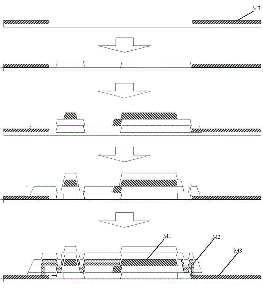
[0024] like figure 1 As shown, the manufacturing method of the flexible display device of the present invention includes the following steps:

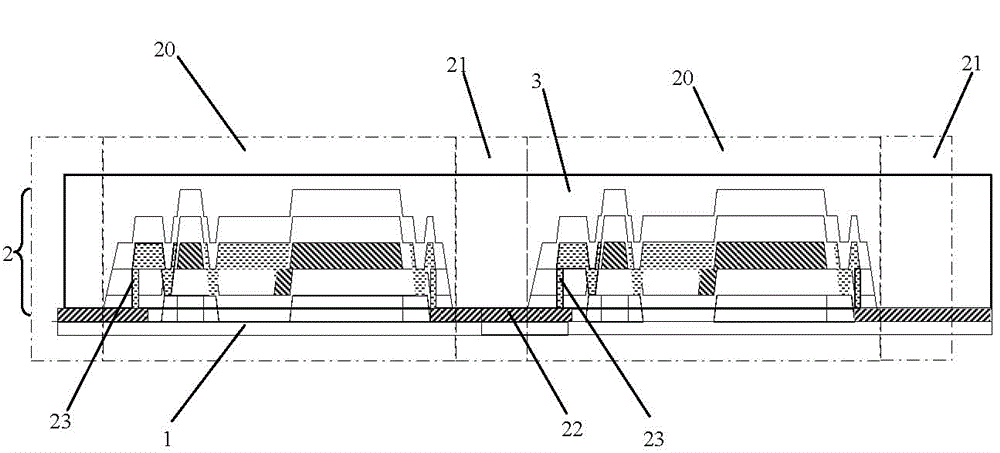
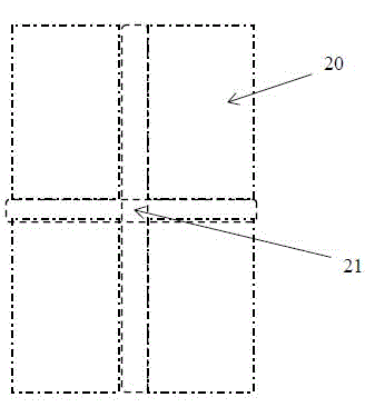
[0025] Step 1. First, divide the flexible substrate into a pixel area and a bending area, and the bending area is divided into multiple rows and columns of pixel areas in the form of rows and columns;

[0026] Step 2, making a metal connection layer M3 in the predetermined bending area (that is, between adjacent pixel areas) on the flexible substrate;

[0027] Step 3: Fabricate TFTs in the pixel area on the flexible substrate, and sequentially fabricate each layer structure of the TFTs;

[0028] Step 4. After the TFT is manufactured, a flattening layer is formed on the bending area between each pixel area and a...


PUM


Abstract

The invention discloses a flexible display device and a making method thereof. The method comprises the following steps: S1, dividing a flexible substrate into pixel regions and a bending region, wherein the bending region spaces the multiple rows of and multiple columns of pixel regions by rows and columns; S2, making a metal connection layer in the bending region of the flexible substrate; S3, making a TFT in the pixel regions of the flexible substrate; S4, after the completion of TFT making, making a flattening layer above the bending region between the pixel regions and above the pixel regions to fill the gaps between the pixel regions with the flattening layer, wherein the metal connection layer is across the flattening layer in the bending region to electrically connect the adjacent pixel regions; and S5, carrying out a subsequent OLED making process. When the flexible display device is bent in the bending region, the stress is concentrated in the bending region, so the risk that the characteristic of the TFT changes or the TFT is broken due to bending of the pixel regions is prevented.

Description

technical field [0001] The present invention relates to a flexible display device and a manufacturing method thereof, in particular to a flexible display device with low cost, large bending degree and not easy to break a thin film transistor and a manufacturing method thereof. Background technique [0002] At present, the structure of each layer of the flexible substrate of the flexible display is inorganic or metal, and the thickness of each layer is similar. Due to the uniform stress distribution during bending, the position of the TFT (Thin Film Transistor, thin film transistor) may be distorted due to the bending characteristics. cause deviation, or even breakage. [0003] In order to solve the above problems, in the prior art, flexible and easy-to-bend materials are often used to manufacture display structures in flexible display devices, such as oxide semiconductors (indium gallium zinc oxide, IGZO) or organic semiconductors (such as copper phthalocyanine , PcCu) and ...

Claims


Application Information

Patent Timeline
Patent Type & Authority Applications(China)
IPC IPC(8): H01L27/32
Inventor 党鹏乐张小宝丁立薇张秀玉袁波
Owner KUNSHAN NEW FLAT PANEL DISPLAY TECH CENT
Why Eureka
Try Eureka