3D stacked structure image sensor reading method based on one-dimensional decoding

An image sensor, stacking structure technology, applied in image communication, image data processing, graphic image conversion, etc., can solve the problems of reduced image quality, unable to read pixel array signals, etc., and achieve the effect of simple connection and wiring

Inactive Publication Date: 2016-08-10
TIANJIN UNIV
View PDF5 Cites 1 Cited by
  • Summary
  • Abstract
  • Description
  • Claims
  • Application Information

AI Technical Summary

Problems solved by technology

Eliminates image quality degradation due to μbump, ADC or TSV failures that prevent signal readout from the entire pixel array

Method used


Image

  • 3D stacked structure image sensor reading method based on one-dimensional decoding
  • 3D stacked structure image sensor reading method based on one-dimensional decoding

Examples


Embodiment Construction

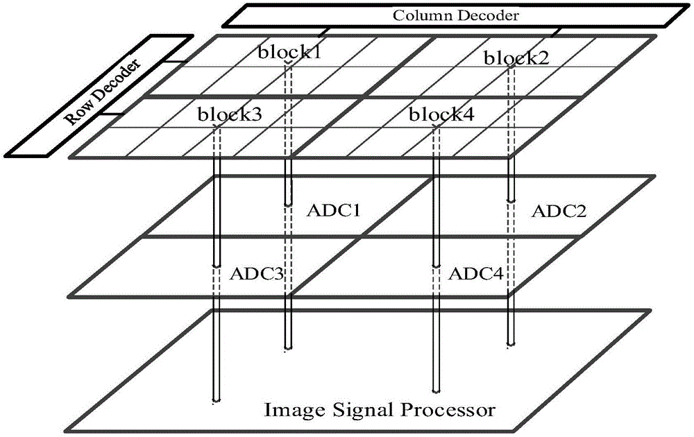
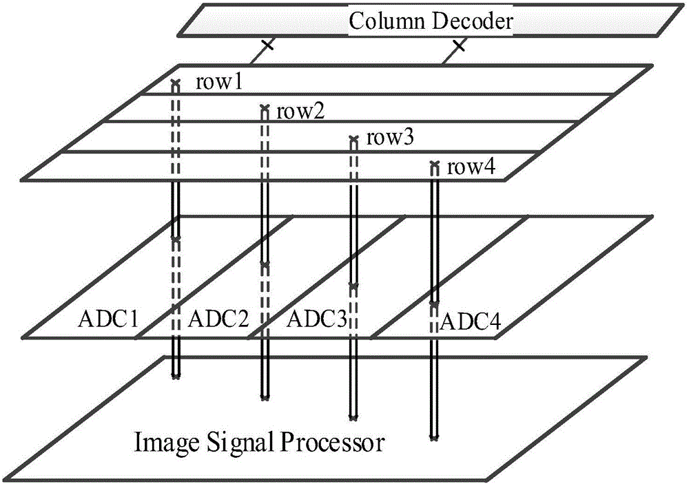
[0010] The image sensor architecture of this design is as follows figure 2 As shown, the pixel array is divided into several sub-processing modules by row (or column), and each row (or column) of pixels in these sub-processing modules is connected to the same ADC through a μbump channel, and each ADC is connected via its own TSV channel to the ISP layer. This connection method makes the row (or column) only need to perform one-dimensional decoding and readout of the column (or row) when the row (or column) is selected and read, and the pixel unit can be a standard 4T unit without adding a selection switch, which simplifies the wiring design of the pixel array. When any part of μbump, ADC or TSV on a pixel signal readout path fails, the ISP will first judge that the pixel readout is abnormal, and use linear interpolation to restore the failed pixel signal value to reduce signal transmission The effect of channel failure on image quality. The linear interpolation algorithm ta...


PUM


Abstract

The invention relates to the technical field of simulation integrated circuit design and the 3D lamination packaging technology and solves a problem of low image quality caused by reading failure of the whole pixel array signal because of mubump, ADC or TSV failure. The method comprises steps that a pixel array is divided into multiple sub processing modules in a mode of the row or the column, pixels of each row or each column of the sub processing modules are connected with one same ADC through a mubump pathway, each ADC is connected with an ISP layer through a respective TSV pathway, so the row or the column is selected to read through only one-dimensional decoding for the row or the column, when the mubump, the ADC or the TSV on a certain pixel signal reading pathway partially fails, the ISP is firstly determined to be abnormal, and failed pixel signal values can be recovered through employing linear interpolation. The method is mainly applied to integrated circuit design manufacturing occasions.

Description

technical field [0001] The invention relates to the technical field of analog integrated circuit design and 3D stack packaging technology, and is an image sensor that simultaneously meets the requirements of innovation, high frame frequency, small size and low cost. Specifically, it relates to a readout method for a 3D stacked structure image sensor. Background technique [0002] 3D stacked structure image sensor (structure such as figure 1 As shown) parallel processing of signals can be realized by utilizing the vertical interconnection between chips of each layer. Compared with the traditional planar CMOS image sensor whose frame rate is limited by the conversion speed of the Analog-to-Digital Converter (ADC), the 3D stacked structure image sensor can double the frame rate while maintaining the same circuit performance. . In the 3D stacked image sensor, the signal collected by the pixel unit is transmitted to the image signal processor (Image Signal Processor, ISP) thro...

Claims


Application Information

Patent Timeline
Patent Type & Authority Applications(China)
IPC IPC(8): H04N5/374H04N5/378G06T3/40
CPCG06T3/4007H04N25/76H04N25/75H04N25/79
Inventor 高静李奕黄蕊贾宬徐江涛史再峰
Owner TIANJIN UNIV
Why Eureka
Try Eureka