Method and device for starting basic input/output system (BIOS)
A consistent, node-based technology, applied in the computer field, can solve problems such as low compatibility of PCIE devices, reduced space, and reduced available memory address space
- Summary
- Abstract
- Description
- Claims
- Application Information
AI Technical Summary
Problems solved by technology
Method used
Image
Examples
Embodiment 1
[0159] see Figure 4 , a BIOS startup method in the embodiment of the present invention is executed by the node, including:
[0160] S401. Enter the first access mode. In the first access mode, the maximum address accessed by the node is the first address; in the first access mode, perform the following steps from S402 to S407;
[0161] In this embodiment, "access mode" refers to a way for a processor (CPU) to address through a bus with a certain number of bits. For example, in the prior art, addressing is usually performed through a 32-bit or 64-bit bus. In this embodiment, the maximum space that can be addressed by the first access mode is smaller than the maximum space that can be addressed by the second access mode to be introduced later. For example, in this embodiment, the first access mode is a 32-bit access mode, that is, addressing is performed through a 32-bit bus, and the maximum addressing space (that is, the "first address" in step S401) is 4GB. Correspondingly, ...
Embodiment 2
[0202] Based on the foregoing embodiments, this embodiment specifically describes step S402 in the first embodiment.
[0203] Exemplary, such as Figure 5 As shown in the example, this node includes 4 CPUs, which are recorded as CPU0, CPU1, CPU2, and CPU3 respectively, and a local MMCFG space of 64 kilobytes (KB) is allocated for each CPU. The allocation results are as follows: CPU0 allocation 2G~2G+64M MMCFG space; CPU1 allocates 2G+64M~2G+64M+64M MMCFG space; and so on for the rest.
[0204] In this way, the local MMCFG spaces of the four CPUs are continuous, and when CPU0 accesses the address of 2G+64M, it will access the MMCFG space of CPU1, and then the Control and Status Register (CSR) register of CPU1 can be operated. When CPU1 accesses the address of 2G, it will access the MMCFG space of CPU0 and operate the CSR register of CPU0. The rest and so on. Realize that any CPU of this node can access the CSR registers of other CPUs in the node.
[0205] Specifically, allo...
Embodiment 3
[0222] Based on the foregoing embodiments, this embodiment specifically describes step S404 in the foregoing embodiments.
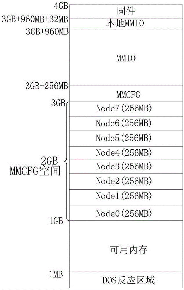
[0223] Exemplarily, the node can allocate the address of the MMCFG space in the global access address by configuring the DRAM Rule register, and can configure the INTERLEAVE_LIST register to set the address of the MMCFG space allocated through the DRAM Rule register in the global access address to the node's MMCFG space.
[0224] Among them, the DRAM Rule register is used for address allocation from the 0MB address to the maximum addressable space of the memory.
[0225] Specifically, by setting the Limit field of the DRAM_RULE_0-19 register to specify the upper limit address of the space, the attr field specifies whether the space is used for DRAM or MMCFG space, and the RULE_ENABLE field specifies whether the rule effectively allocates the memory space of the CPU in the node.
[0226] Exemplarily, the large-scale CC-NUMA system is a 32-way system, the ...
PUM
 Abstract
Description
Claims
Application Information


