OLED (organic light-emitting diode) display panel and preparation method therefor

A technology for display panels and substrates, applied in the field of OLED display panels, can solve the problems of increasing the total optical path of the microcavity, short the total optical path of the microcavity, etc., and achieve the effects of improving the adjustable performance, increasing the total optical path, and high luminous efficiency

Active Publication Date: 2016-08-17
TCL CHINA STAR OPTOELECTRONICS TECH CO LTD
View PDF6 Cites 3 Cited by
  • Summary
  • Abstract
  • Description
  • Claims
  • Application Information

AI Technical Summary

Problems solved by technology

The conventional F-P optical microcavity structure requires two reflective mirrors, and generally adopts a metal-metal structure. Therefore, the total optical path of the microcavity of the F-P optical microcavity structure is limited by the thickness and refractive index of the organic film layer in the OLED display panel. The optical path is short, and it is difficult for industry insiders to increase the total optical path of the microcavity by adjusting the organic film layer in the OLED display panel

Method used


Image

  • OLED (organic light-emitting diode) display panel and preparation method therefor
  • OLED (organic light-emitting diode) display panel and preparation method therefor

Examples


Embodiment Construction

[0037] The following will clearly and completely describe the technical solutions in the embodiments of the present invention with reference to the accompanying drawings in the embodiments of the present invention. Obviously, the described embodiments are only some, not all, embodiments of the present invention. Based on the embodiments of the present invention, all other embodiments obtained by persons of ordinary skill in the art without creative efforts fall within the protection scope of the present invention.

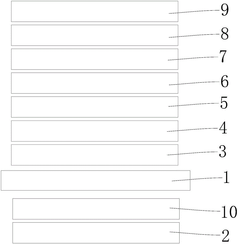
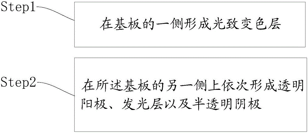
[0038] see figure 1 An embodiment of the present invention provides an OLED (Organic Light-Emitting Diode, Organic Light-Emitting Diode) display panel, including: a substrate 1, a photochromic layer 2, a transparent anode 3 (Anode), a light-emitting layer 6 (Emitting Material Layer) and Translucent cathode 9 (Cathode). Wherein, the photochromic layer 2 is formed on one side of the substrate 1, and the photochromic layer 2 includes a photochromic material that chan...


PUM


Abstract

The invention discloses an OLED (organic light-emitting diode) display panel. The OLED display panel comprises a substrate, a photochromic layer, a transparent anode, an emitting material layer and a semi-transparent cathode, wherein the photochromic layer is formed on one side of the substrate, and includes a photochromic material which changes from a transparent state into a non-transparent state under light excitation; the transparent anode is formed on the other side of the substrate; the emitting material layer is formed on one side, deviating from the substrate, of the transparent anode; the light rays from the emitting material layer comprise wavelengths used for activating the photochromic material; and the semi-transparent cathode is formed on one side, deviating from the transparent anode, of the emitting material layer. The OLED display panel disclosed by the invention has a relatively long micro-cavity total optical length. The invention also discloses a preparation method for the OLED display panel.

Description

technical field [0001] The invention relates to the technical field of OLED display panels, in particular to an OLED display panel and a method for preparing the OLED display panel. Background technique [0002] OLED (Organic Light-Emitting Diode, Organic Light-Emitting Diode) display panel is a new type of display technology developed in the middle of the 20th century. With many advantages such as wide temperature range, low power consumption, low cost, strong shock resistance and flexible display, it will become the main force of the next generation of flat panel display. Its superior performance and huge market potential have attracted many manufacturers and scientific research institutions all over the world to invest in the production and research and development of OLED display panels. [0003] However, due to vibration braiding and inhomogeneous broadening effects, whether it is an organic small molecule or a polymer luminescent material, its spectral half-width is o...

Claims


Application Information

Patent Timeline
Patent Type & Authority Applications(China)
IPC IPC(8): H01L51/52H01L51/56
CPCH10K50/852H10K71/00H10K59/50H10K59/12H10K50/156H10K50/166
Inventor 匡友元
Owner TCL CHINA STAR OPTOELECTRONICS TECH CO LTD
Why Eureka
Try Eureka