

Package structure and package method of blue-light LED flip chip
A packaging structure and flip-chip technology, which is applied in the direction of electrical components, circuits, semiconductor devices, etc., can solve the problems of obvious light spots and affect the lighting effect, and achieve the effect of uniform light output and elimination of light spots
- Summary
- Abstract
- Description
- Claims
- Application Information
AI Technical Summary
Problems solved by technology
Method used
Image

Examples
Embodiment Construction
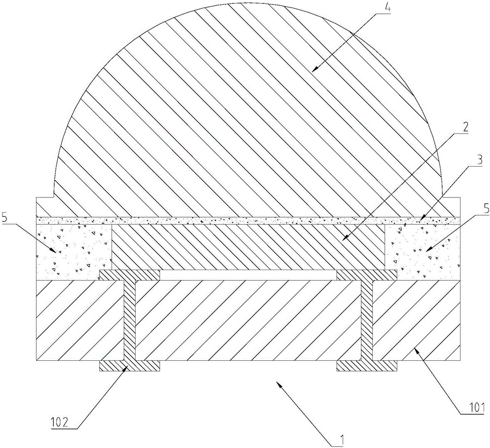
[0025] The structure of the LED lamp bead according to the embodiment of the present invention is as follows: figure 1 As shown, the LED lamp bead of the embodiment of the present invention is packaged by a blue LED flip chip, including a substrate 1 , an LED chip 2 flipped on the substrate, a fluorescent powder adhesive layer 3 , a hemispherical lens 4 and a white reflective adhesive layer 5 . The substrate 1 includes an insulating substrate 101 with pads 102 on the insulating substrate.
[0026] The white reflective adhesive layer 5 surrounds the periphery of the chip 2 , the height of the white reflective adhesive layer 5 is equal to that of the chip 2 , and the fluorescent powder adhesive layer 3 covers the top surface of the chip 2 and the top surface of the reflective adhesive layer 5 . The hemispherical lens 4 is packaged above the phosphor glue layer 3 .
[0027] Wherein, the reflective adhesive layer 5 is made by stirring transparent silica gel and high temperature r...
PUM
 Abstract
Description
Claims
Application Information