
Array substrate and display panel

A technology for array substrates and display panels, applied in optics, instruments, static electricity, etc., can solve problems such as grounding line damage, poor electrostatic protection effect, and grounding line size reduction

Active Publication Date: 2016-08-31
XIAMEN TIANMA MICRO ELECTRONICS +1
View PDF7 Cites 35 Cited by
  • Summary
  • Abstract
  • Description
  • Claims
  • Application Information

AI Technical Summary

Problems solved by technology

[0005] When the electrostatic voltage is large, the existing display panel only discharges the electrostatic charge through the grounding wire 16
The narrow frame design of the display panel is the development trend of the display device, which leads to the narrower width of the frame area of ​​the display panel, which makes the width of the grounding trace 16 continuously smaller, resulting in an increasing impedance of the grounding trace.
When the impedance of the grounding line is large, more heat will be generated when it discharges the electrostatic charge, so that the grounding line 16 is easily broken down and damaged, and the electrostatic protection effect is poor.

Method used


Image

  • Array substrate and display panel
  • Array substrate and display panel
  • Array substrate and display panel

Examples


Embodiment Construction

[0030] The following will clearly and completely describe the technical solutions in the embodiments of the present invention with reference to the accompanying drawings in the embodiments of the present invention. Obviously, the described embodiments are only some, not all, embodiments of the present invention. Based on the embodiments of the present invention, all other embodiments obtained by persons of ordinary skill in the art without making creative efforts belong to the protection scope of the present invention.

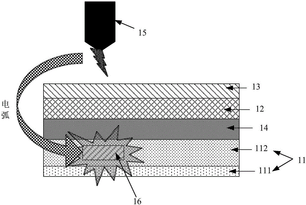
[0031] As mentioned in the background art, in the prior art, static electricity is only discharged through the ground wiring arranged in the frame area. When the electrostatic voltage is too high, the grounding wire is likely to generate a lot of heat during the process of discharging static electricity, and the grounding wire is easily damaged by breakdown, and the static stability protection effect is poor.

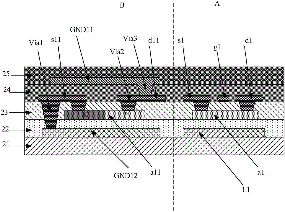
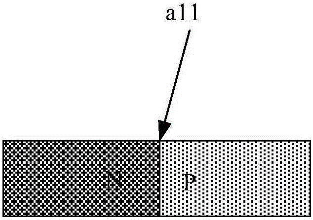
[0032] In order to solve the above problem, an em...


PUM


Abstract

The invention discloses an array substrate and a display panel. The array substrate comprises a transparent substrate, a pixel structure, an anti-static switch tube, a first grounding wire and a second grounding wire, wherein the transparent substrate comprises a display area and a frame area; the pixel structure and the anti-static switch tube are arranged on a same side of the transparent substrate; the pixel structure comprises a pixel thin film transistor; the pixel thin film transistor is positioned in the display area; the anti-static switch tube is positioned in the frame area; the first grounding wire is positioned on one side opposite to the transparent substrate, of the anti-static switch tube; the second grounding wire is positioned between the anti-static switch tube and the transparent substrate; the projections of the first grounding wire and the second grounding wire on the transparent substrate are both positioned on the frame area; the first grounding wire is connected with the second grounding wire through the anti-static switch tube. The array substrate is relatively good in anti-static protection effect.

Description

technical field [0001] The present invention relates to the technical field of display devices, and more specifically, to an array substrate and a display panel. Background technique [0002] With the continuous development of science and technology, more and more display devices are widely used in people's daily life and work, which brings great convenience to people's daily life and work, and has become an indispensable and important display device for people today. tool. The display device performs image display through the display panel. [0003] refer to figure 1 , figure 1 It is a schematic structural diagram of a conventional display panel, which includes: an array substrate 11 and a color filter substrate 12 disposed opposite to each other. Wherein, the array substrate 11 includes a glass substrate 111 and a TFT film layer 112 . The color filter substrate 12 and the array substrate 11 are encapsulated by a sealant 14 . In order to prevent the display panel from...

Claims


Application Information

Patent Timeline
IPC IPC(8): G02F1/1362H05F3/02
CPCG02F1/136204H05F3/02H01L27/0251H01L27/1244H01L27/1218H01L27/0296H01L27/0266H01L29/78678H01L27/1222H01L23/60G02F1/133345G02F1/133514G02F1/1368G02F1/136286G02F1/134309G02F2201/123
Inventor 李元行朱绎桦蔡寿金
Owner XIAMEN TIANMA MICRO ELECTRONICS
Learn More