Silicon-based gas sensitive chip with integrated temperature and humidity sensor and manufacturing method thereof

A humidity sensor, gas-sensitive technology, applied in instruments, scientific instruments, measuring devices, etc., can solve the problem of no integrated gas-sensing unit, and achieve the effect of small size, good process compatibility and high reliability

Inactive Publication Date: 2017-12-19
NO 49 INST CHINESE ELECTRONICS SCI & TECH GRP
View PDF2 Cites 1 Cited by
  • Summary
  • Abstract
  • Description
  • Claims
  • Application Information

AI Technical Summary

Problems solved by technology

[0003] The purpose of the present invention is to solve the problem that the existing silicon-based chips mainly focus on the integration of sensitive units such as temperature, humidity, and pressure, and there is no integrated gas-sensitive unit, and provide two silicon-based gas-sensitive chips with integrated temperature and humidity sensors and its production method

Method used


Image

  • Silicon-based gas sensitive chip with integrated temperature and humidity sensor and manufacturing method thereof
  • Silicon-based gas sensitive chip with integrated temperature and humidity sensor and manufacturing method thereof
  • Silicon-based gas sensitive chip with integrated temperature and humidity sensor and manufacturing method thereof

Examples


specific Embodiment approach 1

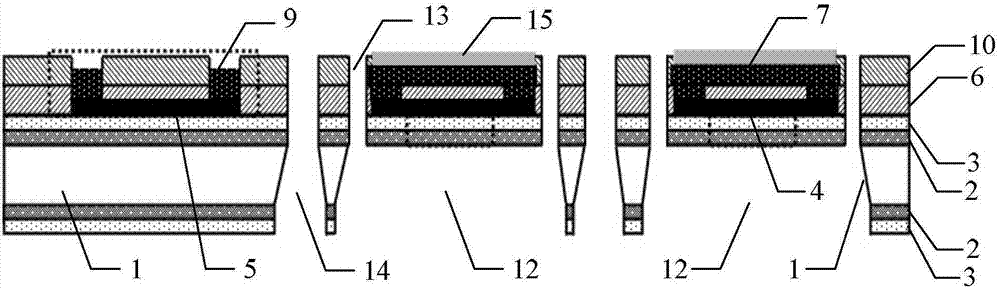
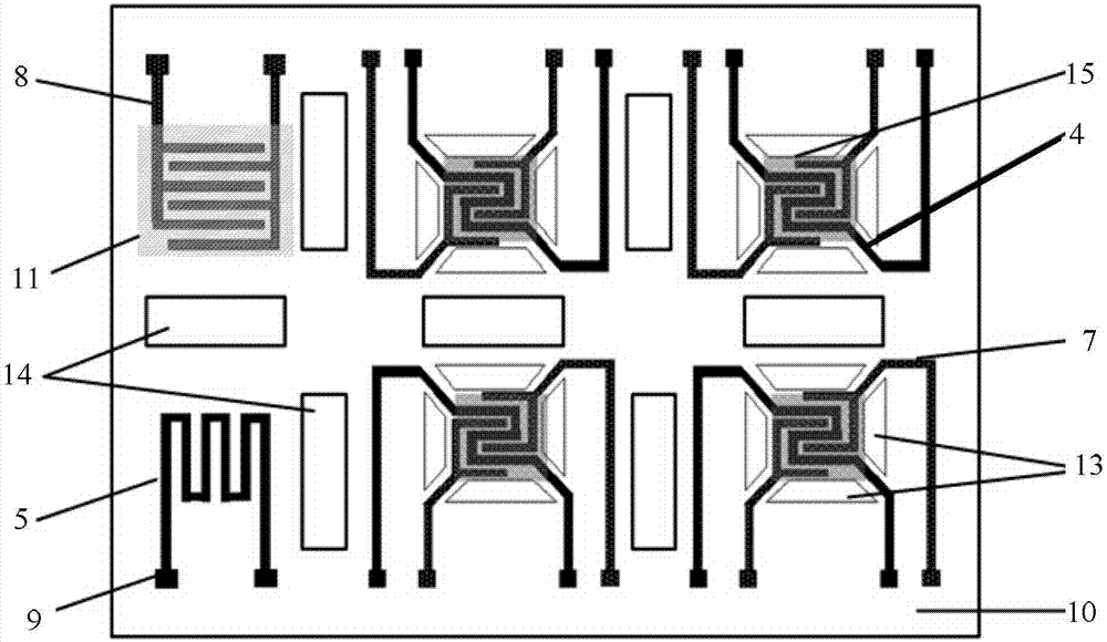
[0022] Specific implementation mode one: the following combination figure 1 , figure 2 and Figure 4 Describe this embodiment mode, the silicon-based gas sensitive chip of integrated temperature and humidity sensor described in this embodiment mode, wherein a plurality of gas sensing units, temperature sensing units and humidity sensing units are all integrated in one N-type (100) single crystal silicon chip Above, a plurality of gas sensing units form an M×N array, M represents the total number of types of gas sensing materials, and N represents the number of gas sensing elements made of each gas sensing material;

[0023] Thermal isolation through holes are arranged between the plurality of gas sensing units, temperature sensing units and humidity sensing units as second-level heat-insulating through-holes, the cross-section of the second-level heat-insulating through-holes is rectangular, and the rectangular The four corners of the arc transition are adopted.

[0024] I...

specific Embodiment approach 2

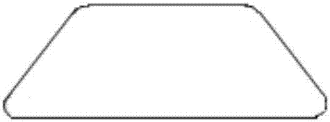
[0030] Specific implementation mode two: the following combination figure 1 , figure 2 and image 3 Describe this embodiment mode. This embodiment mode further defines the silicon-based gas-sensing chip integrated with the temperature and humidity sensor described in Embodiment 1. In this embodiment mode, in the gas sensing unit, each two adjacent electrode leads Each of them is provided with thermal isolation through holes as the first-level heat-insulation through-holes. The cross-section of the first-level heat-insulation through-holes is trapezoidal, and the four corners of the trapezoidal transitions are all made of circular arcs.

[0031] The gas sensing unit is a semiconductor structure of a silicon micro-heating plate, which mainly includes a hollow silicon cup and a micro-heating plate sensing unit formed on it, and the micro-heating plate sensing unit uses silicon dioxide and silicon nitride as a supporting layer, On the support layer are heating electrode leads a...

specific Embodiment approach 3

[0032] Specific implementation mode three: Figure 1 to Figure 4 The specific process of the manufacturing method of the silicon-based gas-sensitive chip integrated with the temperature and humidity sensor described in this embodiment is as follows:

[0033] Step 1. Fabricate a silicon dioxide layer on one surface of the N-type single crystal silicon wafer, and fabricate a silicon nitride dielectric layer on the surface of the silicon dioxide layer, and the silicon dioxide layer and the silicon nitride dielectric layer constitute an induction module (a unit capable of sensing on silicon nitride can be called a sensing module) supporting layer;

[0034] Step 2, making a plurality of heating resistors of the gas-sensing unit and sensitive resistors of the temperature-sensing unit above the support layer, and the plurality of heating resistors form an M×N array;

[0035] Step 3, depositing silicon dioxide or silicon nitride on the support layer as a first insulating passivation ...


PUM


Abstract

The invention provides a silicon-based gas sensitive chip of integrated humiture sensor and a manufacturing method of the silicon-based gas sensitive chip, relating to environment monitoring technology and aiming to solve the problem that a silicon-based chip doesn't have an integrated gas-sensitive unit. A plurality of gas-sensitive units, a temperature sensitive unit, and a humidity sensitive unit are integrated on one N-type monocrystalline silicon wafer, a secondary heat insulation through hole having a rectangular cross section is arranged between every two adjacent units, and in each gas-sensitive unit, a primary heat insulation through hole having a trapezoidal cross section is arranged between every two adjacent electrode lead wires. The four corners of each of the rectangular cross section and the trapezoidal cross section are arranged in an arc transition manner. The chip can monitor the humiture indexes of environment and can monitor various gases, and the two-stage heat insulation can meet the different work temperature requirement of different units. The heat insulation holes are subjected to arc transition instead of sharp angle, so that the array chip has the advantages of multifunctional measurement, good selectivity, high mechanical strength, high reliability, and low power consumption, and is suitable for environment monitoring.

Description

technical field [0001] The invention relates to a silicon-based gas sensitive array chip. Background technique [0002] With the continuous acceleration of urbanization in our country, environmental issues have become one of the important contents that people pay attention to. Realizing accurate monitoring and early warning of urban atmospheric environmental quality has important scientific and social significance. At present, the monitoring of the urban meteorological environment mostly uses discrete instruments, which are expensive and bulky, and are not convenient for in-situ real-time measurement, and cannot obtain meteorological indicators such as temperature and humidity at the same time. With the rapid development of micromachining technology, low power consumption and high performance microsensors become possible. Recently, a small number of micro-gas sensors have appeared on the market, but they can only measure one gas. To measure different gases, different types ...

Claims


Application Information

Patent Timeline
Patent Type & Authority Patents(China)
IPC IPC(8): G01D21/02G01N27/12
CPCG01D21/02G01N27/125
Inventor 王成杨金建东李玉玲丁文波齐虹田雷王明伟夏露郑丽王亚彬
Owner NO 49 INST CHINESE ELECTRONICS SCI & TECH GRP
Why Eureka
Try Eureka