Making method and device for display substrate

A technology of display substrate and manufacturing method, applied in nonlinear optics, instruments, optics, etc., can solve the problems of increasing the design and production cost of APR transfer plate, reducing production capacity, etc., to achieve the effect of saving cost and releasing production capacity

Inactive Publication Date: 2016-09-21
BOE TECH GRP CO LTD +1
View PDF5 Cites 1 Cited by
  • Summary
  • Abstract
  • Description
  • Claims
  • Application Information

AI Technical Summary

Problems solved by technology

In this way, it not only increases the design and production cost of the APR transfer printing plate, but also makes the production line need to frequently replace and clean the APR transfer printing plate, which leads to a reduction in production capacity

Method used


Image

  • Making method and device for display substrate
  • Making method and device for display substrate
  • Making method and device for display substrate

Examples


Embodiment 1

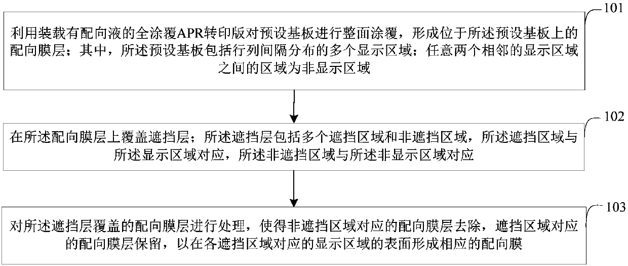
[0039] figure 2 A flow chart of a method for manufacturing a display substrate provided by Embodiment 1 of the present invention is shown. see figure 2 , the method for manufacturing a display substrate provided in Embodiment 1 of the present invention includes the following steps:

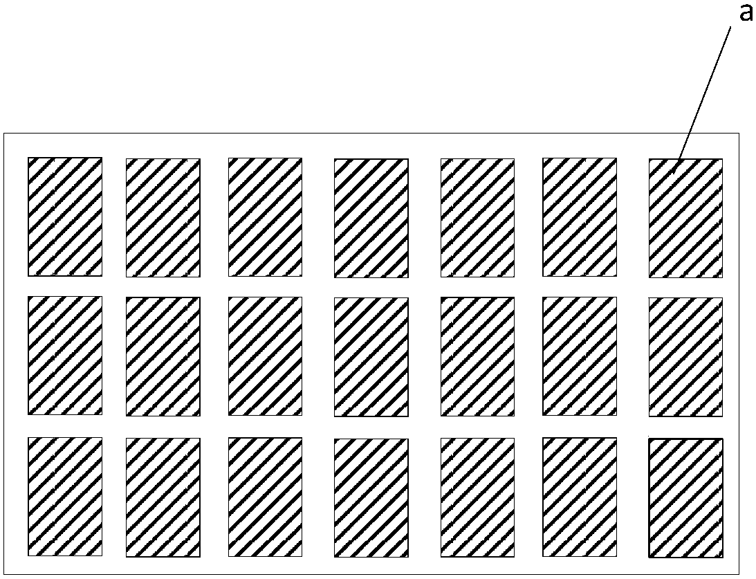
[0040] Step 101: Use the fully coated APR transfer plate loaded with alignment liquid to coat the entire surface of the predetermined substrate to form an alignment film layer on the predetermined substrate; wherein the predetermined substrate includes rows and columns multiple display areas; the area between any two adjacent display areas is a non-display area.

[0041]In this step, the alignment film formed after coating the entire surface of the preset substrate with the fully coated APR transfer plate loaded with alignment liquid is liquid, and the liquid alignment film needs to be pre-cured at this time , the purpose is to remove the solvent in the alignment liquid to make it a solid ali...

Embodiment 2

[0055] Embodiment 2 of the present invention provides a manufacturing device for a display substrate, see Figure 9 , including: a full-coated APR transfer plate 100, a shielding plate 200 and a removal unit 300;

[0056] Wherein, the fully-coated APR transfer plate 100 is used to coat the entire surface of the predetermined substrate after loading the alignment liquid, so as to form an alignment film layer on the predetermined substrate; wherein, the predetermined substrate Including multiple display areas distributed in rows and columns at intervals; the area between any two adjacent display areas is a non-display area;

[0057] The shading plate 200 is used to cover the alignment film layer; the shading plate 200 includes a plurality of shading areas and non-shielding areas, the shading areas correspond to the display areas, and the non-shielding areas correspond to the Corresponding to the non-display area;

[0058] The removing unit 300 is configured to process the alig...


PUM


Abstract

The invention provides a making method and device for a display substrate. The method includes the steps that whole-surface coating is carried out on a pre-arranged substrate through a full-coating APR transfer plate loaded with alignment liquid, and an alignment film layer located on the pre-arranged substrate is formed, wherein the pre-arranged substrate comprises multiple display areas distributed in a row and list spaced mode, and the area between every two adjacent display areas is a non-display area; the alignment film layer is covered with a shielding layer, wherein the shielding layer comprises multiple shielding areas and multiple non-shielding areas, the shielding areas correspond to the display areas, and the non-shielding areas correspond to the non-display areas; the alignment film layer covered with the shielding layer is treated, so that the portions, corresponding to the non-shielding areas, of the alignment film layer are removed, the portions, corresponding to the shielding areas, of the alignment film layer are retained, and thus corresponding alignment films are formed on the surfaces of the display areas corresponding to the shielding areas. By means of the method, different products can share one full-coating APR transfer plate, so that cost is reduced, and productivity is improved.

Description

technical field [0001] The invention relates to the field of display technology, in particular to a method and device for manufacturing a display substrate. Background technique [0002] The specific steps of forming a liquid crystal display box are as follows: first, apply a sealant around one glass substrate, and then add liquid crystals to the center of another glass substrate by dropping method. The two glass substrates are vacuum bonded, and finally the frame sealing glue is cured to complete the box forming process. In the production process of liquid crystal display panels, in order to make the liquid crystal molecules align normally, it is necessary to coat a layer of polyimide film on the surface of the array substrate and color filter substrate, and then perform a rubbing process on the polyimide film to ensure Realize the alignment of liquid crystal molecules. Therefore, the polyimide film coating of the array substrate and the color filter substrate is a very i...

Claims


Application Information

Patent Timeline
Patent Type & Authority Applications(China)
IPC IPC(8): G02F1/1337G02F1/1333
CPCG02F1/13378G02F1/1333
Inventor 周永山覃一锋李建
Owner BOE TECH GRP CO LTD
Why Eureka
Try Eureka