Device and method for transferring two-dimensional layered semiconductor material to diamond anvil cell

A diamond-to-anvil, two-dimensional layered technology, applied in the field of high-voltage devices, can solve the problems of narrow sample chamber, difficulty in cutting substrates, and influence of sample materials

Inactive Publication Date: 2016-09-28
JILIN UNIV
View PDF6 Cites 10 Cited by
  • Summary
  • Abstract
  • Description
  • Claims
  • Application Information

AI Technical Summary

Problems solved by technology

However, the sample cavity of the diamond anvil is very narrow, which makes it very difficult to cut the substrate and put the cut substrate with sample material into the sample cavity.
Moreover, substrates such as silicon wafers and quartz wafers will be greatly deformed under high pressure, which will have a great impact on the sample material.

Method used


Image

  • Device and method for transferring two-dimensional layered semiconductor material to diamond anvil cell
  • Device and method for transferring two-dimensional layered semiconductor material to diamond anvil cell
  • Device and method for transferring two-dimensional layered semiconductor material to diamond anvil cell

Examples


Embodiment 1

[0025] The overall structure of the device for transferring two-dimensional layered semiconductor materials to the diamond counter-anvil of the present invention is described with reference to the accompanying drawings.

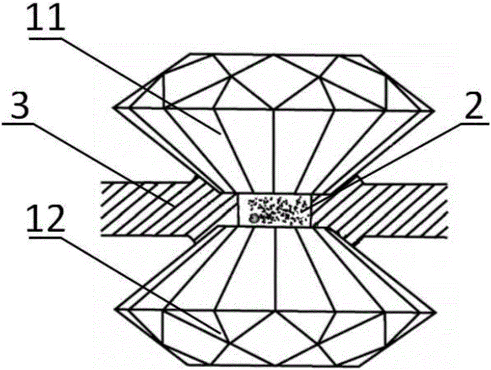
[0026] Such as figure 1 As shown, the diamond counter-anvil is composed of an upper anvil 11, a lower anvil 12, a sample chamber 2, and a metal spacer 3. The upper anvil 11 and the lower anvil 12 are two diamonds, and the metal spacer 3 is generally made of T-301 stainless steel. , There is also a ruby ​​in the sample chamber 2 to calibrate the pressure.

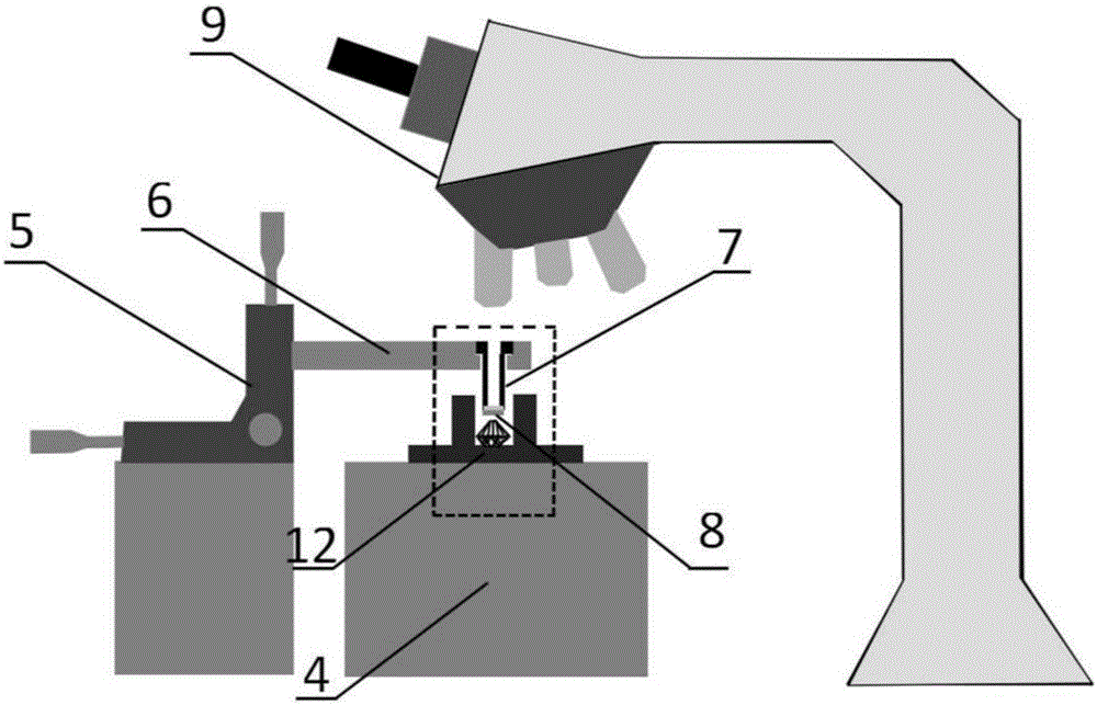
[0027] exist figure 2 Among them, the three-dimensional translation stage 5, the extension arm 6, the vertical shaft 7 and the glass plate 8 constitute the main body of the device for transferring two-dimensional layered semiconductor materials to the diamond anvil; the sample stage 4, optical microscope9.

[0028] Described three-dimensional translation platform 5 selects the three-dimensional translat...

Embodiment 2

[0029] Embodiment 2 transfers two-dimensional layered semiconductor material to DAC

[0030] To transfer the two-dimensional layered semiconductor material into the DAC, the sample material can be directly adhered to the anvil surface of the lower anvil 12 within the sample cavity, and then the diamond is reset so that the sample material is in the sample cavity.

[0031] The adhesive film substrate with the sample of interest is attached to the outer surface of the glass slide 8 at the bottom of the shaft 7 . Such as figure 2 , put the lower anvil 12 on the sample stage 4, use the optical microscope 9 to find the anvil surface of the lower anvil, and move the target position where the target sample is to be transferred to the center of the field of view of the optical microscope 9. The shaft 7 is first positioned above the lower anvil 12, and the adhesive film substrate with the sample is not in contact with the lower anvil 12. Adjust the focal length of the optical micros...

Embodiment 3

[0033]Example 3 Transfer of monolayer MoSe to piston cylinder DAC 2 sample

[0034] In the first step, monolayer MoSe was prepared on the adhesive film substrate by mechanical exfoliation method 2 sample. First cut the adhesive film substrate (model: Gel-Pak PF-30-X4) into 1.5cm 2 Area-sized squares, remove the front and rear protective films, and attach to a clean glass slide. Then a piece of MoSe 2 Put the body material into the tape (Nitto SPV224s), fold and tear the tape in half repeatedly until a layer of samples is evenly distributed on the tape. Cover the tape on the film substrate and tear off the tape. It can be observed that a lot of MoSe remains on the film substrate. 2 Material. Put the film substrate under the optical microscope 9 (eyepiece: 10X objective lens: 50X) to find the sample. After finding the target sample, you can directly perform Raman spectrum characterization and photofluorescence characterization on the film substrate. It is determined that t...


PUM


Abstract

The invention discloses a device and a method for transferring a two-dimensional layered semiconductor material to a diamond anvil cell, and belongs to the technical field of high-pressure devices. The device structurally comprises an optical microscope (9), a sample platform (4), a three-dimensional translation platform (5), an extension arm (6), a silo (7) and a glass piece (8). By adopting the device and the method, the two-dimensional layered semiconductor material can be transferred to the diamond anvil cell, the defects in the prior art that the property of a sample material can be affected as a substrate material is deformed can be avoided, and moreover the technical barrier of electric property measurement on a small amount of two-dimensional layered semiconductor materials under high voltage at present is broken through.

Description

technical field [0001] The invention belongs to the technical field of high-voltage devices, and particularly relates to a device for transferring a two-dimensional layered semiconductor material to a piston cylindrical diamond anvil. Background technique [0002] Since graphene with a two-dimensional hexagonal honeycomb lattice structure was prepared in 2004, its excellent electrical and mechanical properties have attracted extensive attention from researchers in various fields. Since 2010, transition group metal sulfides (in the form of MX2, where M represents group four elements such as Ti, Zr, Hf, etc.; group five elements V, Nb, Ta, etc.; group six elements Mo, W, etc.; X is sulfur group elements, S, Se or Te.) Materials have attracted widespread interest of researchers. The bulk materials of these compounds are composed of layers, the layers are connected by van der Waals force, and the single layer structure is composed of X-M-X. There is a direct band gap in the en...

Claims


Application Information

Patent Timeline
Patent Type & Authority Applications(China)
IPC IPC(8): G01N1/28
CPCG01N1/28
Inventor 周强付鑫鹏李芳菲
Owner JILIN UNIV
Why Eureka
Try Eureka