Built-in touch control substrate, driving method thereof and display panel

An embedded, substrate technology, used in static indicators, optics, instruments, etc., can solve the problem of uneven display and achieve the effect of uniform display

Inactive Publication Date: 2016-09-28
BOE TECH GRP CO LTD +1
View PDF5 Cites 12 Cited by
  • Summary
  • Abstract
  • Description
  • Claims
  • Application Information

AI Technical Summary

Problems solved by technology

[0005] The present invention at least partly solves the problem of uneven display caused by redundant lines in the existing embedded touch substrate, and provides an embedded touch substrate capable of ensuring uniform display, its driving method, and a display panel

Method used


Image

  • Built-in touch control substrate, driving method thereof and display panel
  • Built-in touch control substrate, driving method thereof and display panel
  • Built-in touch control substrate, driving method thereof and display panel

Examples


Embodiment 1

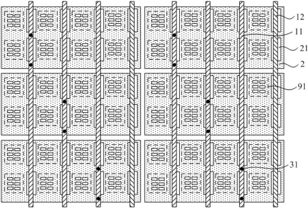
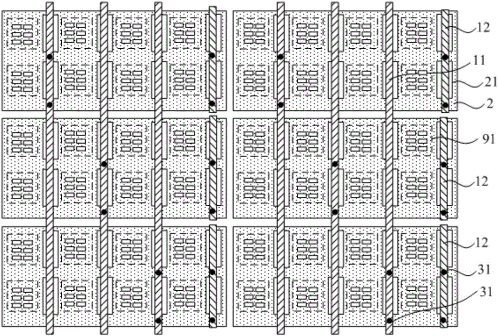
[0035] Such as Figure 2 to Figure 4 As shown, this embodiment provides an in-cell touch substrate.

[0036] The in-cell touch substrate is a substrate in the display panel, but it can also realize the touch function.

[0037] Preferably, the in-cell touch substrate is an array substrate of a liquid crystal display, and thus includes structures such as pixel electrodes, data lines, gate lines, thin film transistors, and gate insulating layers, which will not be described in detail here. Of course, the in-cell touch substrate may also be in other forms such as a color filter substrate.

[0038] Specifically, the above embedded touch substrate includes:

[0039] A plurality of common electrodes, the common electrodes are time-division multiplexed as touch electrodes 2;

[0040] Multiple touch signal lines 11;

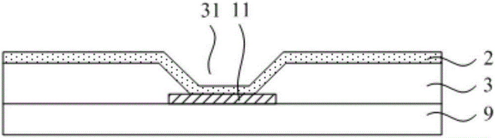
[0041] An insulating layer 3 is provided between the touch electrodes 2 and the touch signal lines 11, and each touch electrode 2 is overlapped with a plurality of to...

Embodiment 2

[0062] This embodiment provides a display panel, which includes:

[0063] The above-mentioned in-cell touch substrate.

[0064] The display panel of this embodiment includes the above-mentioned in-cell touch substrate, so that it has the function of touch control, and the problem of uneven display will not occur.

[0065] Specifically, the in-cell touch substrate can be an array substrate, a color filter substrate, and the like.

[0066] Specifically, the display panel of this embodiment can be any product or component with a display function such as a liquid crystal display panel, an OLED panel, an electronic paper, a mobile phone, a tablet computer, a television set, a monitor, a notebook computer, a digital photo frame, and a navigator.

Embodiment 3

[0068] This embodiment provides a method for driving the above-mentioned in-cell touch substrate, wherein,

[0069] In the display stage, the common electrode signal is applied to the above-mentioned touch signal line to perform display; in the touch stage, the touch signal is applied to the above-mentioned touch signal line to perform touch.

[0070] In this embodiment, since each redundant line is connected to the touch electrode, and the touch electrode is further connected to the touch signal line, when a signal is applied to the touch signal line, the redundant line is also applied through the touch electrode. The same signal, so there is no need to set additional signal sources for the redundant lines, so as not to increase the number of touch chips (that is, not to increase the cost), and to ensure that the signals of the redundant lines are synchronized with the signals of the touch signal lines, thereby playing a role Make the display uniform.


PUM


Abstract

The invention provides a built-in touch control substrate, a driving method thereof and a display panel and belongs to the technical field of touch control. The problem of nonuniform display caused by redundant lines in existing built-in touch control substrates can be solved at least partially. The built-in touch control substrate comprises a plurality of common electrodes and a plurality of touch control signal lines, wherein the common electrodes serve as touch control electrodes through time multiplexing, an insulation layer is arranged between each touch control electrode and the corresponding touch control signal line, and each touch control electrode is superposed with multiple touch control signal lines and electrically connected with one touch control signal line through a via hole in the corresponding insulation layer; furthermore, each touch control electrode is superposed with at least one redundant line, redundant lines superposed with any two different touch control electrodes are insulated from one another, and each touch control electrode is electrically connected with all the redundant lines superposed with the touch control electrode.

Description

technical field [0001] The invention belongs to the field of touch technology, and in particular relates to an embedded touch substrate, a driving method thereof, and a display panel. Background technique [0002] The substrate of the display panel (such as the array substrate) can also be used as a touch substrate, that is, an in-cell touch substrate. An existing in-cell touch substrate such as figure 1 As shown, it includes a plurality of electrodes, each electrode overlaps with a plurality of touch signal lines 11 (there is an insulating layer 3 in between), and is electrically connected to one of the touch signal lines 11 through a via hole 31 in the insulating layer 3 , the touch signal line 11 is connected to the touch chip. In the display stage, the touch signal line 11 inputs a common voltage to the electrodes, and the electrodes are used as common electrodes; That is, the electrodes are time-divisionally multiplexed into common electrodes and touch electrodes 2 ....

Claims


Application Information

Patent Timeline
Patent Type & Authority Applications(China)
IPC IPC(8): G02F1/1333G06F3/041
CPCG02F1/13338G06F3/0412G06F3/0445G06F2203/04111G09G3/36G09G2320/0233
Inventor 肖文俊王春雷
Owner BOE TECH GRP CO LTD
Why Eureka
Try Eureka