Display panel and manufacturing method thereof and display device

A display panel and manufacturing method technology, applied in the direction of instruments, semiconductor devices, optics, etc., can solve the problems of thinness, increased power consumption, loss of light energy, etc., to increase the feasibility of the process, reduce the imaging distance, and transmit rate-boosting effect

Pending Publication Date: 2016-09-28
BOE TECH GRP CO LTD
View PDF6 Cites 13 Cited by
  • Summary
  • Abstract
  • Description
  • Claims
  • Application Information

AI Technical Summary

Problems solved by technology

However, the stacked structure of the backlight module, lower polarizer, array substrate, liquid crystal layer, color filter substrate and upper polarizer in the existing display device limits the thickness of the traditional liquid crystal display device, and it is difficult to make it thinner and thinner.
In addition, the use of color substrates consumes at least 60% of light energy, and can only rely on increasing the brightness of the backlight to meet the brightness requirements of real devices, which undoubtedly increases power consumption

Method used


Image

  • Display panel and manufacturing method thereof and display device
  • Display panel and manufacturing method thereof and display device
  • Display panel and manufacturing method thereof and display device

Examples


Embodiment Construction

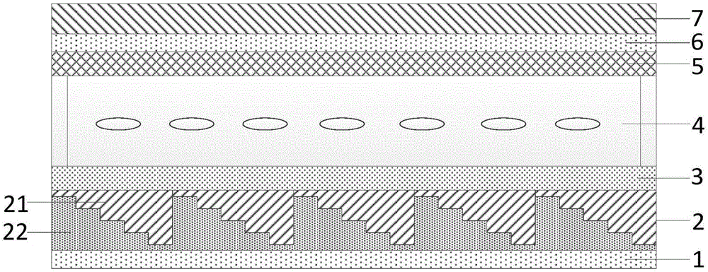
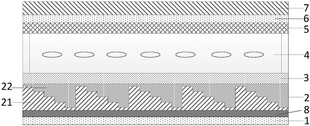
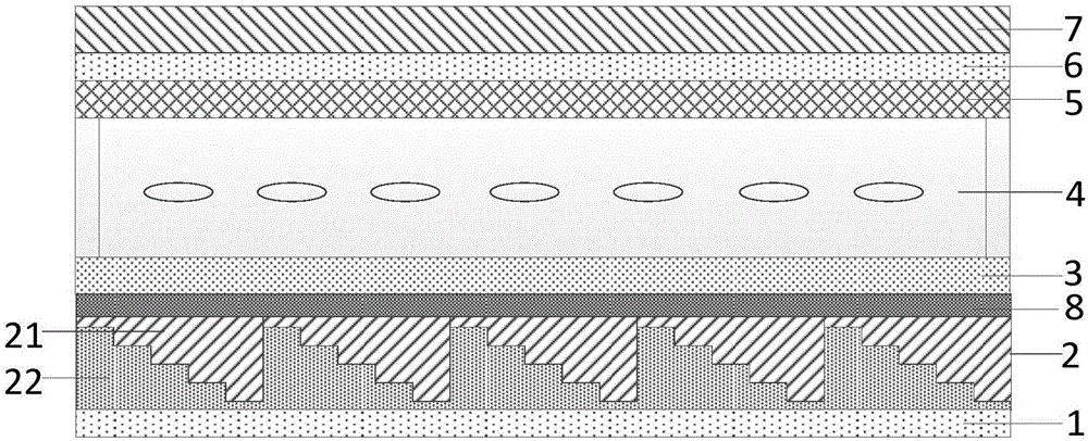
[0077] The following will clearly and completely describe the technical solutions in the embodiments of the present invention with reference to the accompanying drawings in the embodiments of the present invention. Obviously, the described embodiments are only some, not all, embodiments of the present invention. Based on the embodiments of the present invention, all other embodiments obtained by persons of ordinary skill in the art without making creative efforts belong to the protection scope of the present invention.

[0078] figure 1 and figure 2 Schematic diagram of the structure of the display panel in the embodiment of the present invention, as shown in figure 1 , figure 2 As shown, the display panel includes a nano light-splitting film 2 disposed on the side of the array substrate 3 away from the liquid crystal layer 4 .

[0079] Wherein, the nano light-splitting film 2 includes a plurality of light-splitting units arranged in an array, and each light-splitting uni...


PUM

PropertyMeasurementUnit
refractive indexaaaaaaaaaa

Abstract

The embodiment of the invention provides a display panel and a manufacturing method thereof and a display device. The display panel comprises a nano light splitting film arranged between an array substrate and a first Polaroid. The nano light splitting film comprises a plurality of light splitting units distributed in an array, and each light splitting unit corresponds to at least one sub-pixel unit. Each light splitting unit comprises a multi-order grating structure and is used for splitting light corresponding to at least one sub-pixel unit to obtain light in one or more preset colors. A nano light splitting element is applied to the display panel so that a color film layer of a liquid crystal display device can be omitted, transmittance of the liquid crystal display device is increased, and color quality of the display device is improved on the condition that cost is not greatly increased.

Description

technical field [0001] The invention relates to the technical field of liquid crystal display, in particular to a display panel, a manufacturing method thereof, and a display device. Background technique [0002] With the rapid development of technology in the display field, people have higher and higher requirements for display devices. Thinness, convenience, energy saving, delicate picture, cost reduction, and diversified functions are always the development goals of display devices. However, the stacked structure of the backlight module, lower polarizer, array substrate, liquid crystal layer, color filter substrate and upper polarizer in the existing display device limits the thickness of the traditional liquid crystal display device, making it difficult to make it thinner. In addition, the use of color substrates consumes at least 60% of the light energy, and the only way to meet the brightness requirements of real devices is to increase the brightness of the backlight,...

Claims


Application Information

Patent Timeline
Patent Type & Authority Applications(China)
IPC IPC(8): G02F1/1335
CPCG02F1/133504G02F1/133528H01L27/14692G02F1/133514G02F2202/36G02F2201/305G02F1/133H10K50/865H10K59/35H01L27/0214H01L27/1214
Inventor 谭纪风杨亚锋
Owner BOE TECH GRP CO LTD
Why Eureka
Try Eureka