

Array substrate and display panel
An array substrate and the same technology are applied in the field of display devices, which can solve the problems of low brightness and low aperture ratio of display panels, and achieve the effects of large pixel aperture ratio, increased display area space, and increased aperture area.
- Summary
- Abstract
- Description
- Claims
- Application Information
AI Technical Summary
Problems solved by technology
Method used
Image

Examples
Embodiment Construction
[0024] The following will clearly and completely describe the technical solutions in the embodiments of the present invention with reference to the accompanying drawings in the embodiments of the present invention. Obviously, the described embodiments are only some, not all, embodiments of the present invention. Based on the embodiments of the present invention, all other embodiments obtained by persons of ordinary skill in the art without making creative efforts belong to the protection scope of the present invention.
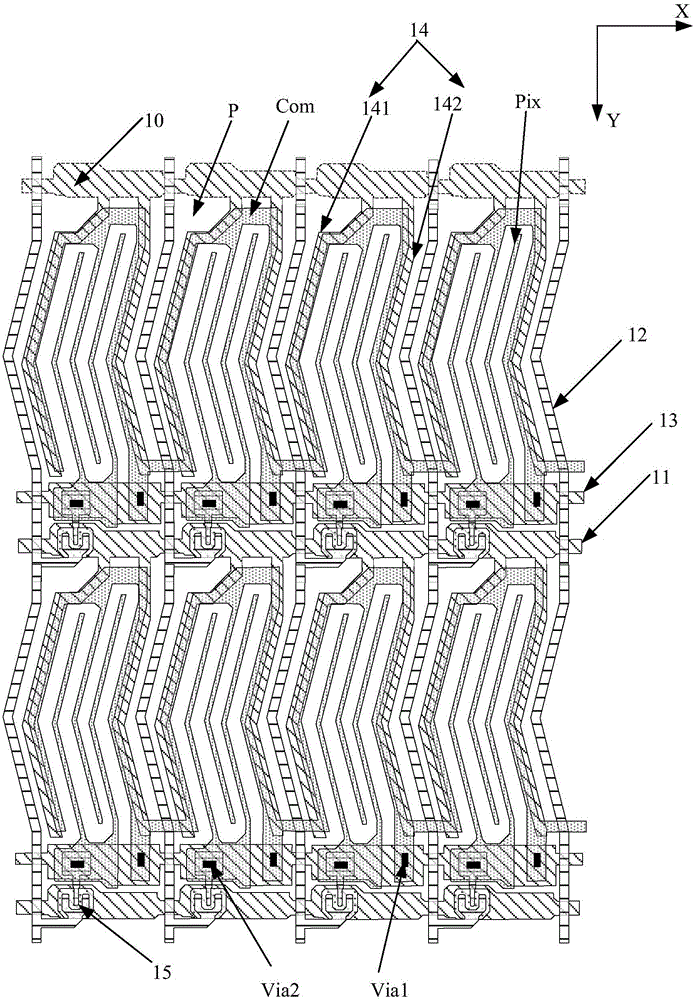
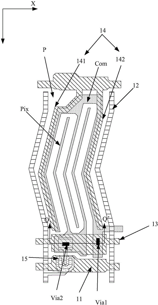
[0025] In a traditional IPS display panel, each row of pixel units requires two common wirings, and all pixel units in the row of pixel units are located between the two common wirings. One of the common wirings is used to provide preset voltage signals to all common electrodes of the pixel units in the row, and the other common wiring is used to form storage capacitors with the pixel electrodes of the pixel units, and the storage capacitors are used for displa...
PUM
 Abstract
Description
Claims
Application Information