

Display panel and preparation method thereof and display device
A display panel and display area technology, which is applied in semiconductor/solid-state device manufacturing, instruments, electrical components, etc., can solve problems such as easy breakage or peeling of circuit structure wiring, poor display of display panels, etc.
- Summary
- Abstract
- Description
- Claims
- Application Information
AI Technical Summary
Problems solved by technology
Method used
Image

Examples
preparation example Construction
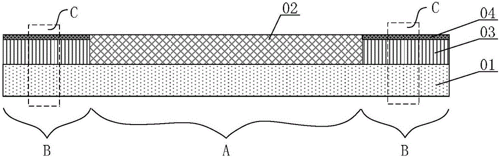
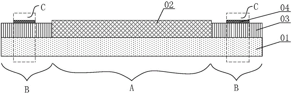
[0050] An embodiment of the present invention provides a method for preparing a display panel. The display panel includes such as figure 2 Shown in display area A and non-display area B, as figure 1 As shown, the preparation method of the display panel includes:
[0051] S101, such as figure 2 As shown, the non-display area B where the peripheral circuit 03 is formed is divided into a bent area C, and at least the protective layer 04 covering the peripheral circuit 03 is formed in the bent area C.
[0052] It should be noted that the display panel also includes a display area A. In this case, in order to realize the screen display function of the display panel, a display device layer 02 is also formed on the base substrate 01 of the display panel at a position corresponding to the display area A. , the display device layer 02 can be an OLED device layer (Organic Light Emitting Diode, organic light emitting diode), or a liquid crystal display device layer, which can be sele...
Embodiment 1
[0088] Before the non-display area B formed with the peripheral circuit 03 is divided into the bending area C (step S101), the preparation method is as follows: Figure 7 shown, also includes:
[0089] S201, such as Figure 8a As shown, the first substrate 011 is disposed at least in the display area A.
[0090] S202 , disposing the second substrate 012 in the non-display area B.
[0091] S203 , splicing the first substrate 011 and the second substrate 012 to form the base substrate 01 of the display panel, and the second substrate 012 is made of a flexible material.
[0092] In this way, if Figure 8a As shown, the base substrate 01 is formed by splicing the first substrate 011 and the second substrate 012, wherein the second substrate 012 disposed in the non-display area B is made of a flexible material, so as to at least achieve the purpose of bending the second substrate 012 .
[0093] The first substrate 011 is at least disposed in the display area A, which may be as...
Embodiment 2
[0107] Before the non-display area B formed with the peripheral circuit 03 is divided into the bending area C (step S101), as Figure 10 As shown, the preparation method also includes:
[0108] S301, such as Figure 11 As shown, the second substrate 012 is arranged in the non-display area B and the display area A;
[0109] S302. Attach the first substrate 011 to the upper surface of the second substrate 012 at a position corresponding to the display area A to form the base substrate 01 of the display panel. The second substrate 012 is made of a flexible material.
[0110] In this way, the base substrate 01 includes a second substrate 012 and a first substrate 011 disposed on the upper surface of the second substrate 012 corresponding to the display area A, wherein the first substrate 011 can be directly pasted on the upper surface of the second substrate 012 , can also be fixedly arranged on the upper surface of the second substrate 012 in other ways, and the connection way ...
PUM
 Abstract
Description
Claims
Application Information