Semiconductor package with heat sink

a technology of semiconductors and heat sinks, applied in the field of semiconductor packages, can solve the problems of increasing the overall height and generating more heat, so as to avoid cracking at the connecting surface of the substrate and the heat sink, and preventing cracking. , the effect of affecting the reliability of the semiconductor packag

Inactive Publication Date: 2005-10-18
UTAC HEADQUARTERS PTE LTD
View PDF7 Cites 8 Cited by
  • Summary
  • Abstract
  • Description
  • Claims
  • Application Information

AI Technical Summary

Benefits of technology

[0009]The semiconductor package of the present invention involves positioning a semiconductor chip and a heat sink, respectively, on two sides of the opening formed in the substrate, and fully filling a thermally conductive adhesive therebetween. The difficulties of the semiconductor packaging process in the prior art that inserts a heat sink into a substrate and the cracking at the connecting surface of the substrate and the heat sink are prevented, avoiding cracking induced by the effect of thermal stress generated during thermal cycling and reliability testing, due to the difference between the coefficients of thermal expansion of the substrate and the heat sink, which allows the humidified air to enter the package through the cracks between the substrate and the heat sink, affecting the reliability of the semiconductor package. Moreover, through the thermally conductive adhesive applied between the semiconductor chip and the heat sink, the heat generated in the semiconductor chip may be directly transferred to the heat sink through a heat dissipation path kept to a minimum length. Further, when the finished semiconductor package is soldered to the printed circuit board, the heat sink is hidden in the gap between the bottom of the chip and the printed circuit board created by the second electrically conductive elements. Thus, the addition of a heat sink will not increase the overall height of the finished package. Moreover, electromagnetic shielding is provided by the heat sink between the semiconductor chip and the printed circuit board, thereby enhancing electromagnetic shielding of the semiconductor and reducing electromagnetic interference. As a result an end product having better electrical properties is fabricated.

Problems solved by technology

However, the more devices and circuitry that are integrated on a semiconductor chip, the more heat that is generated.
Although the method for wrapping the heat sink into the molding compound helps to enhance the heat dissipation rate, it increases the overall height of the semiconductor package.
This thermally conductive path is too long and, moreover, the heat needs to pass through molding compound having a low heat dissipation rate, It is thus very hard to enhance the overall heat dissipation rate of this idea.
This increases the requirements of manufacturing precision and difficulties during operation.
Moreover, since the coefficient of thermal expansion of the substrate and the coefficient of thermal expansion of the heat sink are often significantly different from each other, the effect of thermal stress during a thermal cycle and a reliability test may induce cracking at the connecting surface of the substrate and the heat sink.
Humidified air may thus enter inside the package through the gap formed between the substrate and the heat sink and affect the reliability of the semiconductor package.

Method used


Image

  • Semiconductor package with heat sink
  • Semiconductor package with heat sink
  • Semiconductor package with heat sink

Examples


Embodiment Construction

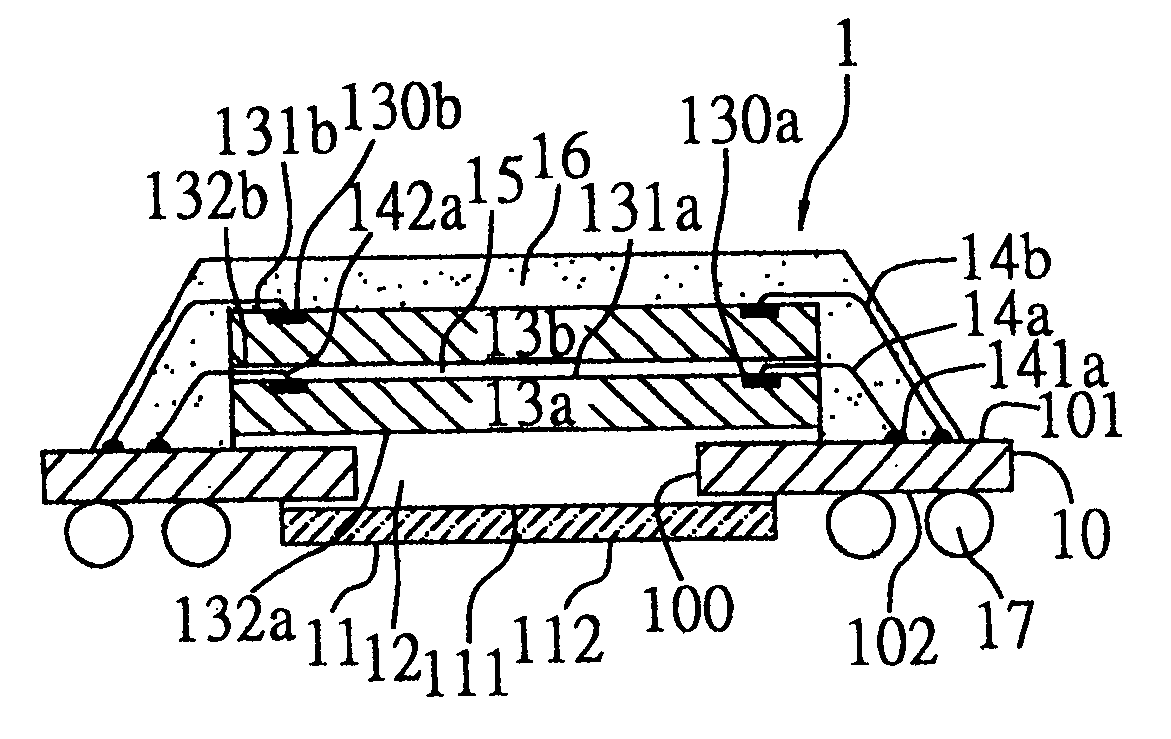
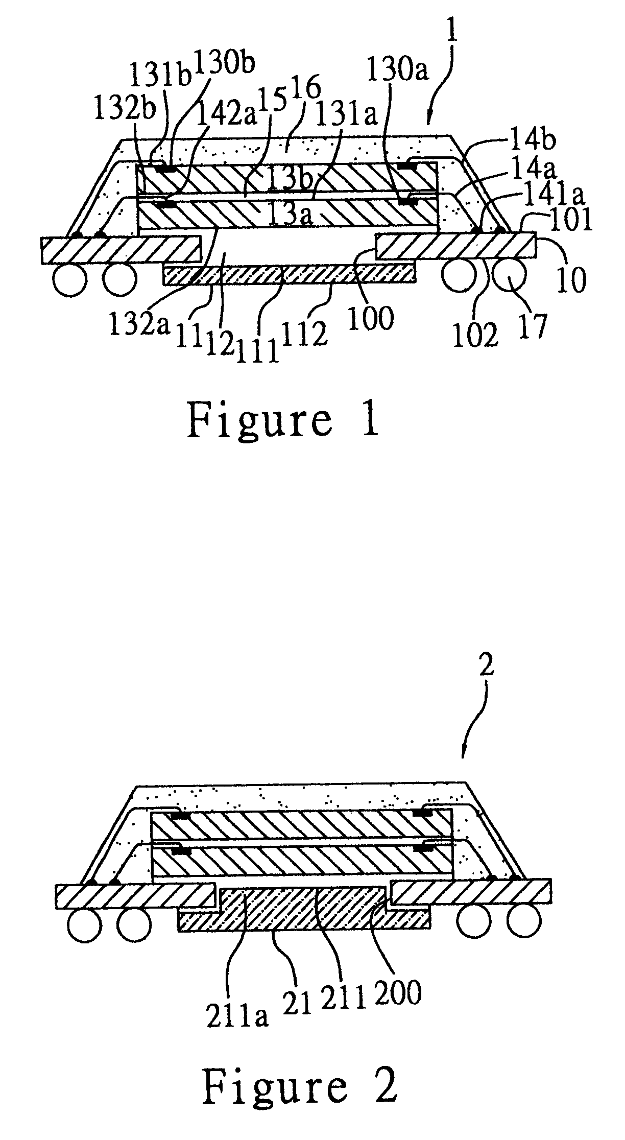
[0014]FIG. 1 is a cross-sectional diagram of a semiconductor package, in accordance with one embodiment of the present invention.

[0015]As shown, the semiconductor package 1 is a Window Ball Grid Array (Window-BGA) package having many chips, which comprises: a substrate 10, on which at least one opening 100 is formed; a heat sink 11, for closing one side of the opening 100 formed on the substrate; a thermally conductive adhesive 12, which is applied on the heat sink 11 for adhesively connecting heat from the heat sink 11 on the surface of the substrate 10; a first chip 13a, which is adhesively connected to the other side of the heat sink corresponding to the opening 100 formed on the substrate, with the thermally conductive adhesive 12 fully filling the space between the first chip 13a and the heat sink 11; a plurality of first bonding wires 14a, which enables the first chip 13a to electrically connect with the substrate 10; a second chip 13b, which is adhesively connected to the fir...


PUM


Abstract

A semiconductor package with a heat sink is provided, having a substrate formed with at least one opening penetrating therethrough. A heat sink is mounted on a surface of the substrate same as for forming solder balls and seals one end of the opening by a thermally conductive adhesive. At least one chip is mounted on the other surface of the substrate opposite to the heat sink via the thermally conductive adhesive and covers the other end of the opening. The thermally conductive adhesive is filled in the opening between the substrate and the heat sink and allows heat produced by the chip to be dissipated through a shorter thermally conductive path. By the above arrangement with the heat sink being mounted between the chip and an external device, the heat sink provides electromagnetic shielding between the chip and the external device and enhances electrical performance of the semiconductor package.

Description

FIELD OF THE INVENTION[0001]The present invention relates to semiconductor packages, and more particularly, to a semiconductor package with a heat sink so as to enhance the heat dissipation rate of the semiconductor package.BACKGROUND OF THE INVENTION[0002]The reason why a Ball Grid Array (BGA) package has become a mainstream of the package products these days is mainly because of its sufficient provision of I / O connections to meet the demands of semiconductor chips on which a high density of devices and circuitry is integrated. However, the more devices and circuitry that are integrated on a semiconductor chip, the more heat that is generated. Without dissipating the heat generated by the semiconductor chip in a timely manner, the life and performance of the semiconductor chip will be greatly reduced.[0003]In order to solve the above-mentioned drawbacks, the idea of adding a heat sink into a semiconductor package has thus arisen. The technique is to wrap the semiconductor chip toge...

Claims


Application Information

Patent Timeline
Patent Type & Authority Patents(United States)
IPC IPC(8): H01L23/34H01L23/367H01L23/31H01L23/28H01L25/065
CPCH01L23/3128H01L24/32H01L25/0657H01L23/3677H01L2924/01087H01L2224/32057H01L2224/32188H01L2224/32225H01L2224/48091H01L2224/48227H01L2224/73265H01L2224/83385H01L2924/01029H01L2924/01047H01L2924/15311H01L2924/3025H01L2924/15151H01L2225/06565H01L2225/06589H01L2225/0651H01L24/48H01L2924/01033H01L2924/00014H01L2924/00H01L2924/3512H01L2224/05599H01L2224/45099H01L2224/85399H01L2924/181H01L2924/351H01L2924/00012H01L2224/45015H01L2924/207
Inventor SU, HUAN-PING
Owner UTAC HEADQUARTERS PTE LTD
Why Eureka
Try Eureka