
Method for quality testing and analysis of tube core of GaAs-based semiconductor quantum dot laser

A detection method and laser technology, applied in the direction of semiconductor lasers, single semiconductor device testing, lasers, etc., can solve the problems of small amount of information, complex equipment, high testing costs, etc., and achieve the effect of strong comparison and easy mastery

Inactive Publication Date: 2008-07-02
INST OF SEMICONDUCTORS - CHINESE ACAD OF SCI
View PDF0 Cites 9 Cited by
  • Summary
  • Abstract
  • Description
  • Claims
  • Application Information

AI Technical Summary

Problems solved by technology

Although the DLTS method can detect the types of defects and related parameters in materials, it is beneficial to study related physical problems, but it requires variable temperature tests, which takes a long time, the equipment is relatively complicated, and the operation is relatively complicated
Although the general PL method is relatively simple and fast, for samples with a quantum dot laser structure, an infrared excitation light source must be used, and small changes in the optical path, the stability of the intensity of the excitation light source, the cleanliness and flatness of the sample surface, etc. The light intensity has a great influence, and the amount of information related to the quality of the material available is small
The TEM method can only be used for the study of line dislocations, and cannot detect invisible defects such as point defects, and has the disadvantages of difficult sample preparation and high testing costs.
The I-V characteristic method is a common method to detect the reverse characteristics of p-i-n diodes, but it can only indirectly reflect the quality of the material, and the reverse characteristics of the diode are greatly affected by the growth of P-layer and N-layer materials, end-face leakage and subsequent processes. Big

Method used


Image

  • Method for quality testing and analysis of tube core of GaAs-based semiconductor quantum dot laser
  • Method for quality testing and analysis of tube core of GaAs-based semiconductor quantum dot laser
  • Method for quality testing and analysis of tube core of GaAs-based semiconductor quantum dot laser

Examples


Embodiment

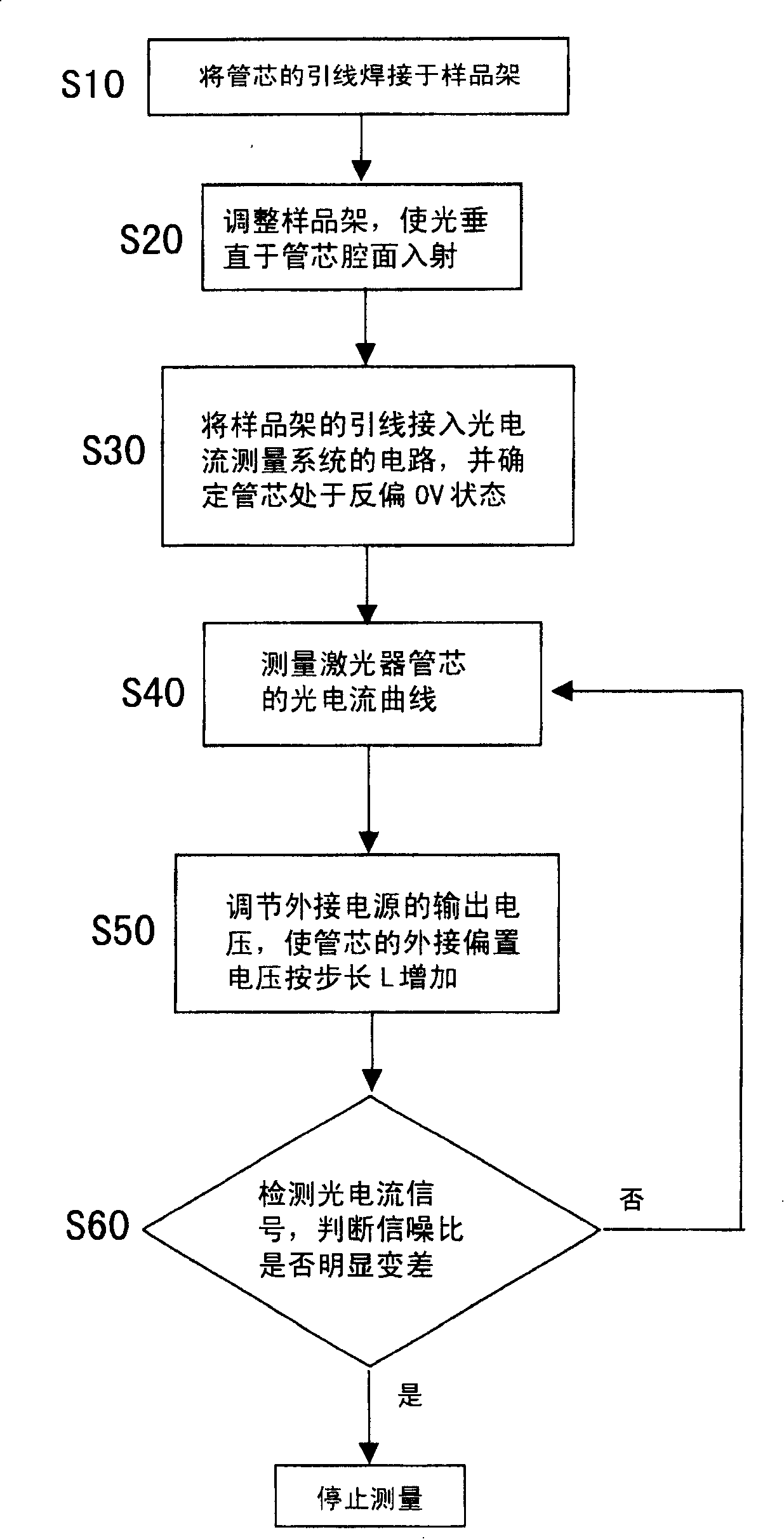
[0060] see again figure 1 and figure 2 Shown, the detection method of a kind of GaAs base semiconductor quantum dot laser die quality of the present invention:

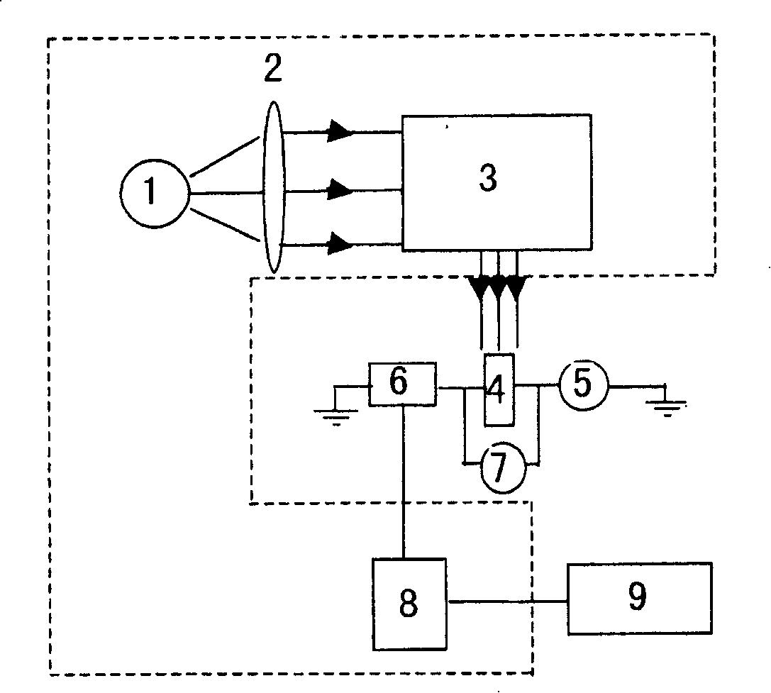
[0061] 1, adopt measuring method described in the present invention ( figure 1 )and figure 2 device shown. Among them, the tungsten lamp 1, the lens group 2, the Michelson interferometer 3, and the data acquisition circuit 8 are the main components of the Fourier transform infrared spectrometer. Finished product, its structure and operation method will not be repeated here. 4 is the laser die to be measured, 5 is the voltage source (for adding reverse bias to the laser die and providing the power supply of the preamplifier), 6 is the preamplifier (for small signal amplification), and 7 is the voltmeter (use Voltage monitoring at both ends of the tube core), and 9 is a computer (for the control and data processing of the Fourier infrared spectrometer).

[0062] 2. The measurement process of the photocurrent cur...


PUM


Abstract

The invention relates to a detection method for the quality of a laser tuber core of GaAs-based semiconductor quantum point. The invention is characterized by comprising the following steps: step 1, a lead wire of the laser tube core is welded on a sample shelf; step 2, the sample shelf is adjusted to cause the light to shine in vertical to the laser tube core; step 3, the lead wire of the sample shelf is accessed in the circuit of the photocurrent of the detection system and determines that the laser tube core is in the state of reverse bias 0V; step 4, the photocurrent curve of the laser tube core is detected; step 5, the output voltage of the external power is adjusted to increase the external connection offset voltage of the tube core according to the step L; step 6, the signal-to-noise ratio is detected. If the signal-to-noise ratio is detected and an obvious negative change is found, the detection is stopped immediately. If no negative change happens, the step 4 is then repeated.

Description

technical field [0001] The invention relates to a method for detecting and analyzing the quality of a tube core of a GaAs-based semiconductor quantum dot laser. More precisely, it is an optimized analysis method for detecting the quality of GaAs-based semiconductor quantum dot laser dies and related data by using photocurrent spectroscopy with light incident vertically on the cavity surface. Background technique [0002] Because the confined electrons and photons in the nano-quantum structure present many physical connotations that are very different from those in the bulk material structure, and are very rich in new quantum phenomena and effects, this also provides new opportunities for the development of electronic and optoelectronic devices with new principles. Opportunities, such as the development of quantum wells, quantum wires and quantum dot lasers, modulators and detectors based on different application goals and working in different wavelength bands, etc., have man...

Claims


Application Information

Patent Timeline
Patent Type & Authority Applications(China)
IPC IPC(8): H01S5/00H01S5/343H01L21/66G01R31/26
Inventor 梁凌燕叶小玲徐波陈涌海王占国
Owner INST OF SEMICONDUCTORS - CHINESE ACAD OF SCI
Learn More